




fig11
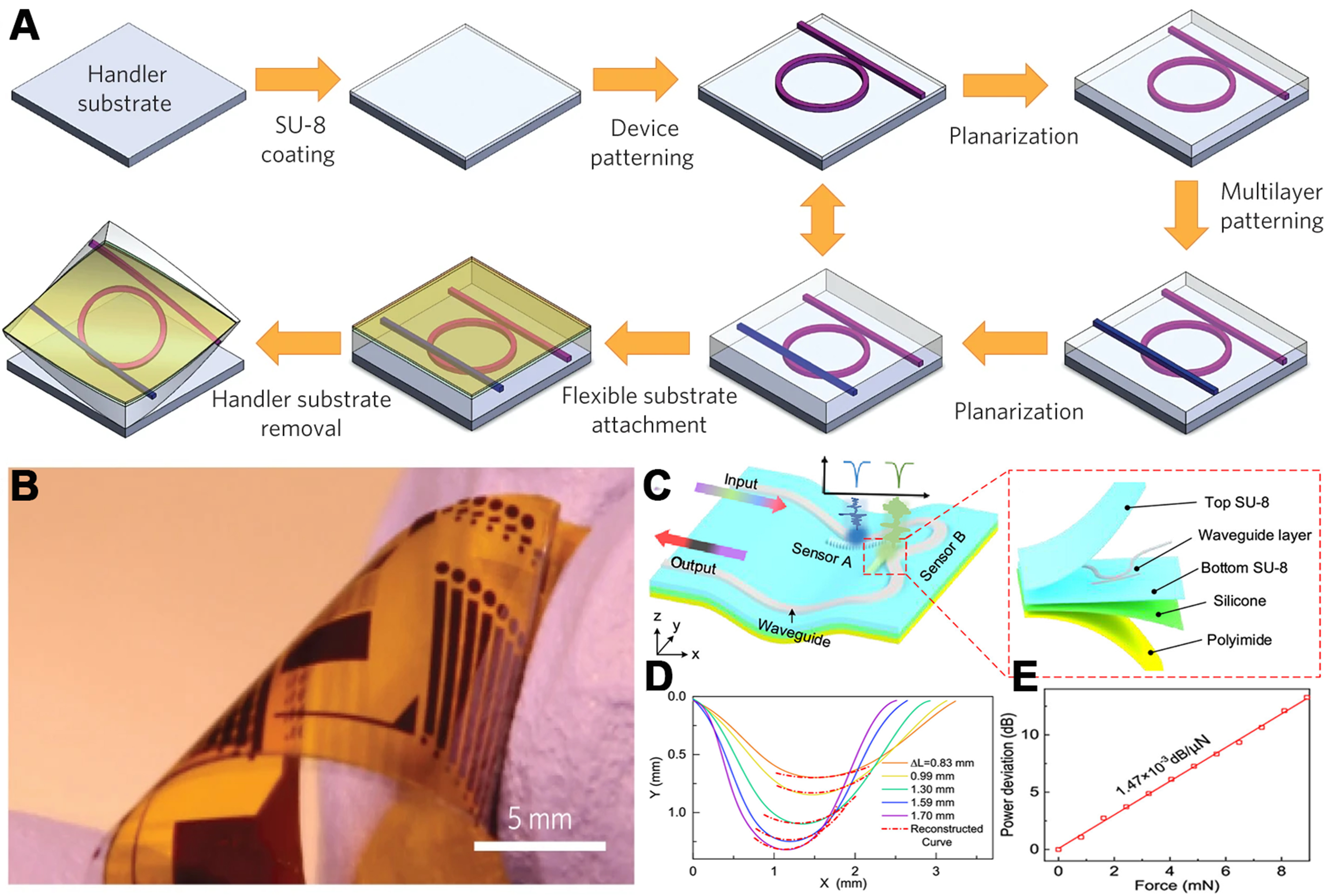
Figure 11. Flexible glass photonic device fabrication and applications[117]: (A) Schematic diagram of the device fabrication process; (B) Photograph of a flexible photonic chip. (A and B) are reprinted with permission from Ref.[117], Copyright © 2014 Springer Nature. Flexible ChG waveguide integrated strain sensors[105]: (C) Schematic of the flexible sensors; (D) Cross-sectional bending curves of the buckling chip under microscope observation (solid lines) and reconstructed by cascaded sensors (dotted lines) for different moving distances; (E) Relationship between the received optical power deviation and force applied on the sensor. (C-E) are reprinted with permission from Ref.[105], Copyright © 2023 American Chemical Society. ChG: Chalcogenide glass.