

Direct Z-scheme siloxene germanane nanosheet heterojunctions for broadband photodetection and ultrasensitive photoelectrochemical sensing
 0
0 Graphical Abstract
Abstract
Siloxene and germanane are two-dimensional (2D) direct-bandgap semiconductors that hold promise for a range of applications, including photocatalysis, electronics, and photodetectors (PDs). In this study, we explore a novel direct Z-scheme 2D-2D siloxene/germanane heterojunction fabricated via wet-mixing self-assembly. This heterojunction exhibits superior light absorption compared with the individual nanosheets. Notably, when employed as a photoelectrode material for photoelectrochemical (PEC) PDs, it shows a marked photoresponse across the 365-980 nm range, with a peak responsivity at 520 nm. Specifically, under 520 nm illumination, its responsivity surpasses those of siloxene and germanane nanosheets by factors of 221.3 and 3.7, respectively. Remarkably, even at zero bias, it achieves a high photoresponsivity of 3.75 μA W-1 and a detectivity of 1.3 × 10⁸ Jones, demonstrating excellent self-powered performance. Owing to its exceptional light sensitivity at 520 nm, the Z-scheme heterojunction is particularly well suited for the PEC photodetection of tartrazine, offering an ultralow detection limit of 0.3 pM and a broad linear range from 1 pM to 1 μM in aqueous media. Overall, this research highlights the considerable potential of the siloxene/germanane heterojunction for advanced optoelectronic applications, including high-performance PDs and PEC sensors.
Keywords


 Download PDF
INTRODUCTION
In recent years, two-dimensional materials (2D) have attracted widespread attention due to their unique properties and broad application prospects. 2D materials such as MXene, phosphorene, silicene, germanene and transition metal dichalcogenides have been extensively used in optoelectronic devices, solar cells, photoelectrochemical (PEC) sensors, and gas sensors[1-5]. They possess a large specific surface area, high electron mobility, abundant active sites, and efficient carrier separation capabilities. Among these materials, siloxene and germanane are particularly noteworthy for their excellent electronic and optoelectronic properties[6]. They are derivatives of 2D silicene and germanene, both of which have a honeycomb-like 2D structure similar to that of graphene. The difference is that the atoms in the honeycomb skeleton are not coplanar, but adopt a buckled structure. Siloxene is composed of silicon, oxygen, and hydrogen atoms, with hydrogen atoms and hydroxyl groups covalently bonded to the upper and lower surfaces of the honeycomb-like silicene[7]; germanane is composed of germanium and hydrogen atoms, with hydrogen atoms covalently bonded to the upper and lower surfaces of the honeycomb-like germanene framework[8]. Both siloxene and germanane exhibit direct bandgap semiconducting properties and good visible-light absorption[9]. They also possess abundant surface-active sites, high theoretical carrier mobility, and tunable bandgap structures, rendering them suitable for transistors[10,11], photodetectors (PDs)[12,13], metal-ion batteries[14-16], capacitors[17,18], electrochemical sensors[19-23], as well as various photocatalytic and photoelectrocatalytic applications[23-29].
However, the photoelectric performance of siloxene and germanane when used individually may be limited by the recombination of photogenerated electrons and holes. Siloxene's wide bandgap (approximately
Recently, Z-scheme heterojunctions have attracted considerable attention due to their ability to simultaneously achieve efficient charge separation and strong redox capability[36-38]. In a Z-scheme system, the photogenerated electrons in the conduction band of one semiconductor recombine with the holes in the valence band of the other, leaving the electrons with stronger reducing power and the holes with stronger oxidizing power at their respective sides[39,40]. This charge transfer pathway not only suppresses carrier recombination but also preserves the maximum redox potentials for both reduction and oxidation reactions. Various Z-scheme heterojunctions based on 2D materials, such as g-C3N4/MXene[41], TiO2/MoS2[42], and WO3/g-C3N4[43], have been reported for photocatalytic and PEC applications. However, to the best of our knowledge, there have been no reports on the electronic and optical properties of siloxene/germanane heterojunctions and their applications in optoelectronic devices.
PEC PDs and sensors are key components of advanced sensing technologies[44,45]. PDs convert light signals into electrical signals, whereas PEC sensors employ light to drive electrochemical reactions, enabling the detection of specific analytes. Both technologies are essential for the development of sensitive and efficient detection methods in areas such as food safety and environmental monitoring[46-50]. The presence of food additives poses a significant public health concern. Traditional detection methods, such as ultraviolet-visible (UV-vis) spectroscopy, fluorescence emission spectroscopy, high-performance liquid chromatography, and gas chromatography, often suffer from drawbacks such as long reaction times, costly equipment, high detection costs, and complex procedures[51]. Therefore, there is an urgent need for convenient, accurate, and low-cost food safety detection methods. PEC sensors employ light as the excitation source and photocurrent as the detection signal, offering rapid response, high sensitivity, low cost, and flexibility, and thus exhibiting great promise for various applications[52,53]. As a key component of PEC sensors, the performance of photosensitive materials plays a decisive role in determining the sensitivity, selectivity, and stability of the sensor.
In this study, we prepared germanane nanosheets (GeNSs) and siloxene nanosheets (SiNSs) via liquid-phase exfoliation using polyvinylpyrrolidone (PVP) as a surfactant, and subsequently assembled them into GeNSs/SiNSs nanocomposites through liquid-phase assembly. The structural, electronic, and optoelectronic properties of the resulting heterojunctions were systematically investigated through a combination of theoretical calculations, materials characterization, and PEC measurements. Particular attention was paid to the heterojunction formation mechanism, charge transfer dynamics, and the resulting photoresponse performance. Furthermore, we explored the potential application of the GeNSs/SiNSs heterojunction as a PEC photosensitive material for the detection of food additives, specifically tartrazine, as a model analyte. This work aims to demonstrate the feasibility of constructing high-performance, self-powered PEC PDs and ultrasensitive sensors based on 2D/2D germanane/siloxene heterojunctions.
EXPERIMENTAL
Preparation of layered 2D/2D GeNSs/SiNSs nanocomposites
GeNSs/SiNSs nanocomposites were prepared via wet-mixing self-assembly of few-layer GeNSs and SiNSs. The resulting nanocomposites were designated H1, H2, and H3 for mass ratios of GeNSs to SiNSs of 1:9, 3:7, and 1:1, respectively. The few-layer GeNSs and SiNSs were obtained through ultrasonic exfoliation assisted by PVP solution. Germanane and siloxene were synthesized following the literature[8,27]. Detailed procedures are provided in the Supplementary Materials.
Photoelectrochemical measurements
Photoelectrochemical measurements were performed at room temperature using an electrochemical workstation equipped with a three-electrode cell. Illumination was provided by a 300 W xenon lamp and monochromatic light at 365, 405, 520, 635, 750, 808, and 980 nm to irradiate the working electrode, and the corresponding light intensities were designated as Level I, II, III, and IV [Supplementary Table 1]. Detailed procedures are described in the Supplementary Materials.
PEC detection of tartrazine
A three-electrode system consisted of an Indium tin oxide (ITO)/GeNSs-SiNSs heterostructure electrode as the working electrode, a Pt plate as the counter electrode and a saturated calomel electrode (SCE) as the reference electrode. Under
RESULTS AND DISCUSSION
2D/2D GeNSs/SiNSs nanocomposites were prepared by a facile ultrasonication-centrifugation process and a liquid-phase assembly technique, as shown in Figure 1. The results of atomic force microscopy (AFM) characterization show that the thickness of GeNSs ranges from 3.5 to 4 nm [Supplementary Figure 1A], while the thickness of SiNSs ranges from 1.5 to 2 nm [Supplementary Figure 1B], indicating that the exfoliated nanosheets are few-layer nanosheets; notably, the size of GeNSs is apparently larger than that of SiNSs. The Fourier transform infrared (FTIR) spectra [Supplementary Figure 1C] indicate that GeNSs/SiNSs nanocomposites exhibit clear main characteristic peaks of pure germanane and siloxene. Raman spectra [Supplementary Figure 1D] also indicate that all characteristic Raman peaks of both germanane and siloxene can be observed in GeNSs/SiNSs nanocomposite samples.
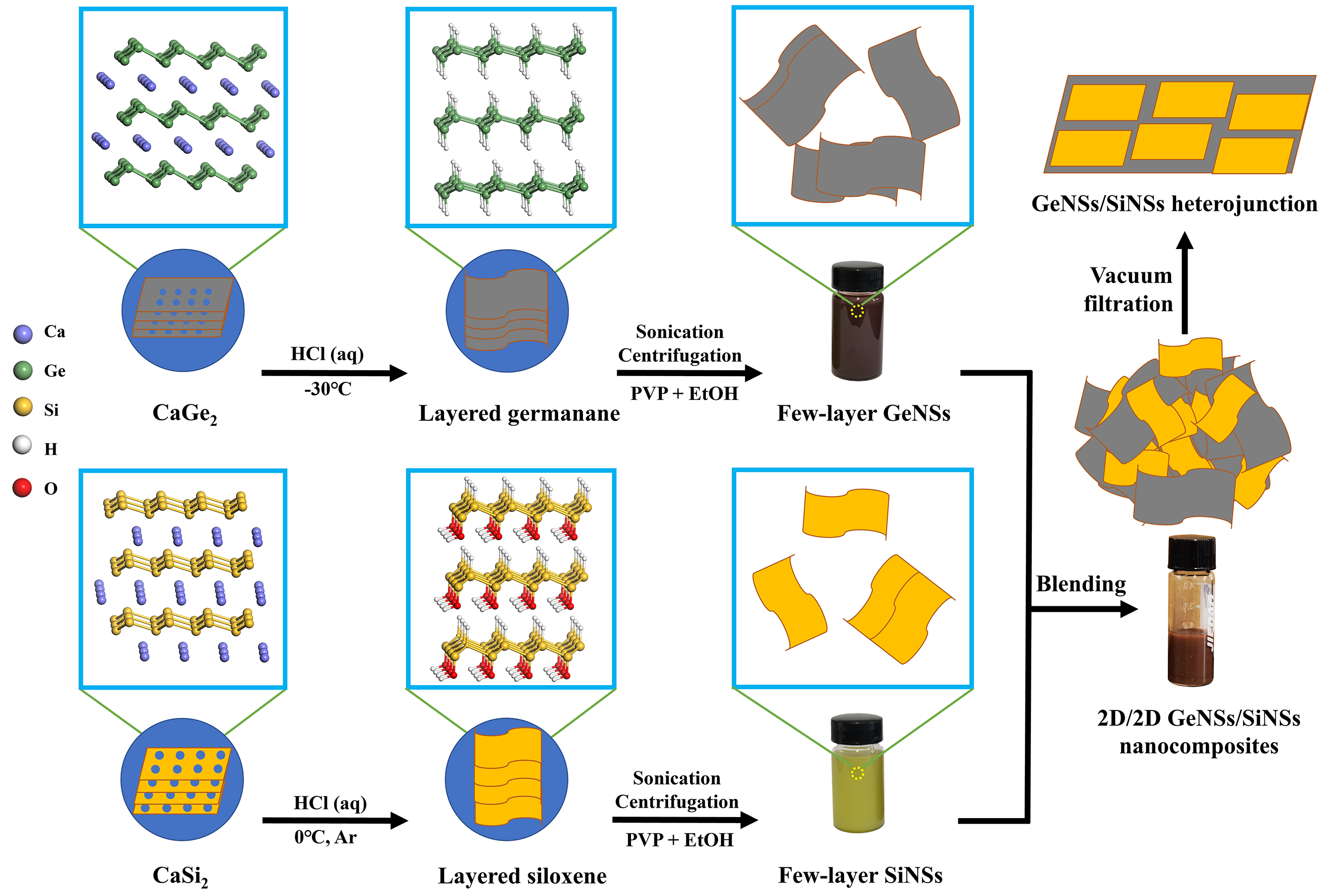
Figure 1. Schematic diagram of preparation process of 2D/2D GeNSs/SiNSs nanocomposites.
Supplementary Figure 1E shows the crystal structure of GeNSs/SiNSs nanocomposites. Due to the amorphous nature of siloxene[17,18,25,54], no obvious diffraction peaks of siloxene were observed in the GeNSs/SiNSs composite, while the characteristic diffraction peaks of germanane are clearly displayed in the GeNSs/SiNSs composite. However, the difference is that the peak position at around 15° representing the interlayer spacing of germanane varies slightly. This is because SiNSs and GeNSs are stacked together, resulting in a change in the interlayer spacing of the composites. The X-ray diffraction, FTIR, and Raman results demonstrate that in GeNSs/SiNSs composites, GeNSs and SiNSs are physically stacked together via van der Waals interactions.
Figure 2A and B show scanning electron microscope (SEM) images of SiNSs and GeNSs obtained by exfoliation. The average size of SiNSs is about 365 nm, while that of GeNSs is about 574 nm, and the size distribution of SiNSs is relatively more uniform, whereas the overall size of GeNSs is larger than that of SiNSs. After the assembly of GeNSs and SiNSs, a three-dimensional stacked structure is formed, as shown in Figure 2C. Because the transmission electron microscope (TEM) morphology of GeNSs and SiNSs is very similar, it is difficult to clearly distinguish them based solely on morphology [Figure 2D]. Through the high-resolution TEM (HRTEM) characterization of the nanosheets in the dark blue dotted circles [Figure 2E], clear lattice fringes and amorphous structures can be observed, respectively.
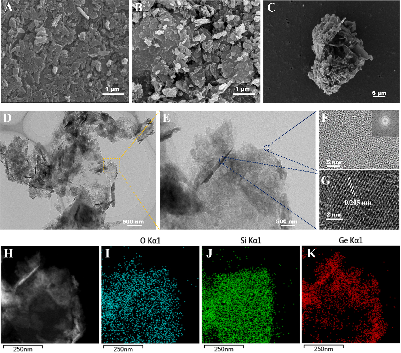
Figure 2. (A-C) SEM images of (A) SiNSs, (B) GeNSs and (C) H2 nanocomposites; (D) TEM image of H2 nanocomposites, (E) HRTEM of H2 nanocomposites; (F) HRTEM image of the dark blue circle in (E), inset is the corresponding fast Fourier transform (FFT) pattern; (G) HRTEM image of the yellow circle in (E), inset is the corresponding fast Fourier transform (FFT) pattern. (H-K) STEM image of the GeNSs/SiNSs composites (H) with its corresponding EDS elemental mapping of (I) O, (J) Si, and (K) Ge elements.
The lattice fringes are characteristic of GeNSs, and the amorphous regions are characteristic of SiNSs, which is consistent with the fast Fourier transform (FFT) patterns (insets in Figure 2F and G). Scanning transmission electron microscope (STEM)
To investigate the surface composition and chemical state of the heterostructure, we conducted X-ray photoelectron spectroscopy (XPS) characterization, as shown in Figure 3. The XPS survey spectra for the heterostructure shown in Figure 3A confirmed the presence of Ge, Si, and O, consistent with the results obtained from energy dispersive spectrometry (EDS) mapping. The high-resolution Ge 3d XPS spectrum of GeNSs in Figure 3B revealed four peaks at 28.39, 28.91, 29.54, and 30.76 eV. The peak at 28.39 eV corresponds to Ge-Ge bonds in elemental Ge[57]. The peaks at 28.91 and 29.54 eV are attributed to the Ge 3d5/2 and Ge 3d3/2 components of GeNSs[58], respectively. The weaker peak at 30.76 eV is likely due to Ge-O bonds resulting from the surface oxidation of GeNSs[14]. For SiNSs, the Si 2p XPS spectrum in Figure 3C was deconvoluted into two peaks at 99.9 and
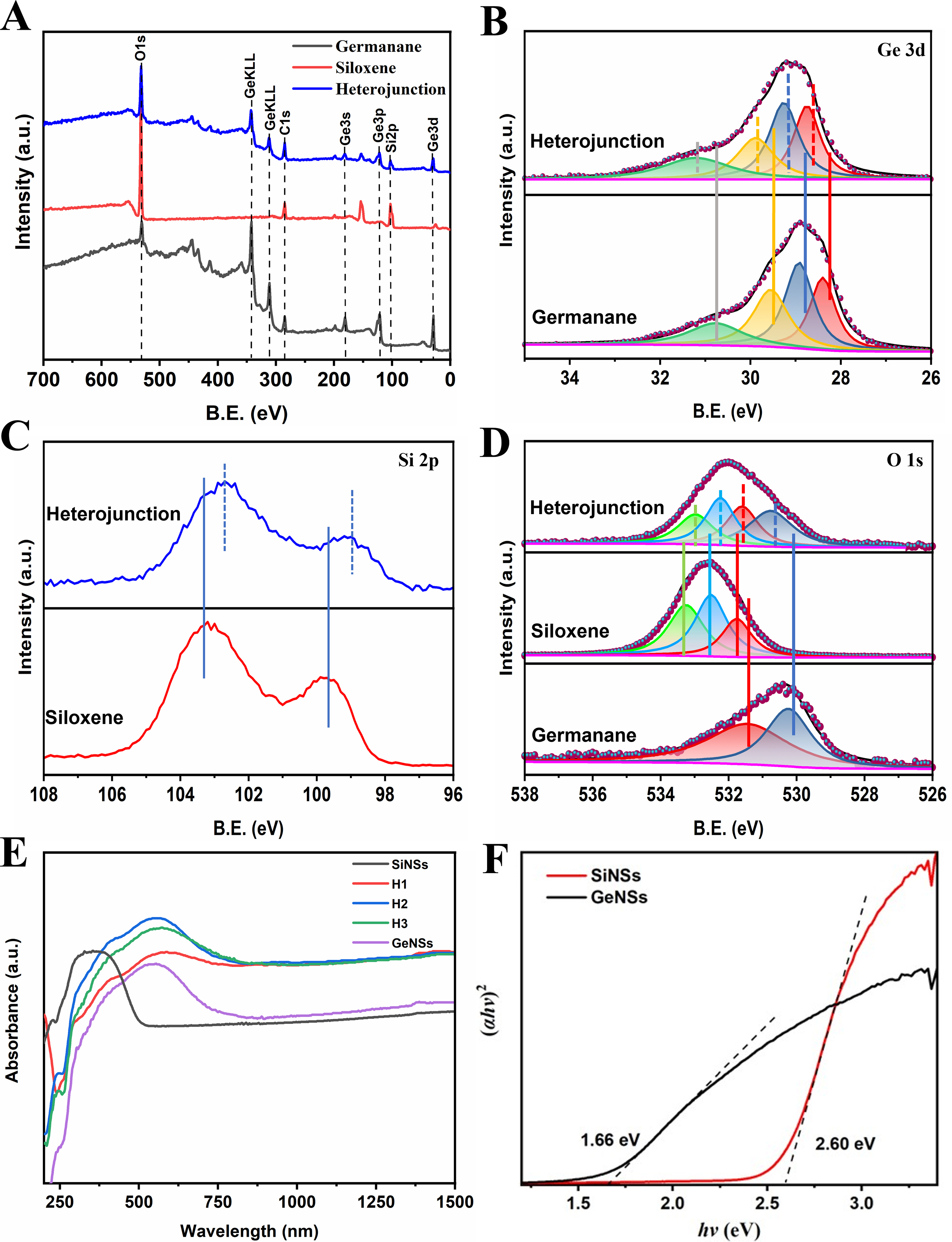
Figure 3. XPS spectra of germanane, siloxene and GeNSs/SiNSs heterostructure. (A) Survey spectra, (B) Ge 3d, (C) Si 2p and (D) O 1s. (E) UV-vis-NIR absorption spectra of GeNSs, SiNSs, and GeNSs/SiNSs H1, H2, and H3. (F) Tauc plot diagram of GeNSs and SiNSs.
The O 1s XPS spectra of the GeNSs/SiNSs heterostructure [Figure 3D] were fitted to four peaks at 530.8, 531.6, 532.2, and 533.0 eV. The peaks at 532.2 and 533.0 eV are assigned to Si-O bonds and the surface oxygen from hydroxyl groups, respectively, originating from SiNSs. The peak at 530.8 eV corresponds to Ge-O bonds from GeNSs. Importantly, the peak at 531.6 eV, originating from both GeNSs (531.5 eV) and SiNSs (531.76 eV), corresponds to adsorbed oxygen species, indicating the presence of oxygen vacancies in both materials, as confirmed by our previous work[27]. These oxygen vacancies could enhance the separation of photoexcited charge carriers and extend the light response into the visible and near-infrared regions (NIR), thus improving photoreactivity[61,62]. Additionally, we observed positive shifts in the O 1s binding energies for GeNSs and negative shifts for SiNSs within the heterostructure, consistent with the shifts in the binding energies of Ge 3d and Si 2p. This further corroborates the formation of the GeNSs/SiNSs heterostructure with strong interaction between the two components[35].
Figure 3E presents the UV-vis-NIR spectra of pure GeNSs, SiNSs, and GeNSs/SiNSs heterojunctions H1, H2, and H3. SiNSs exhibit an absorption onset at around 476 nm, whereas GeNSs show broad light absorption across the UV, visible, and even NIR regions, with enhanced absorption between 400 and 700 nm. The incorporation of GeNSs into SiNSs extends the absorption range from nearly 500 nm to over 800 nm, with enhanced absorption intensity in the visible region, attributed to the synergistic effect between SiNSs and GeNSs[63,64]. The increase in photoexcited charge carriers was further demonstrated by subsequent photocurrent measurements. Figure 3F displays the classical Tauc plots, revealing band gaps of 2.60 eV for SiNSs and 1.66 eV for GeNSs, which are in close agreement with reported values[12,25,65].
To assess the photoresponse performance, SiNSs, GeNSs, and heterojunctions H1, H2, and H3 were fabricated into photoelectrodes, and their PEC properties were evaluated in a three-electrode system with
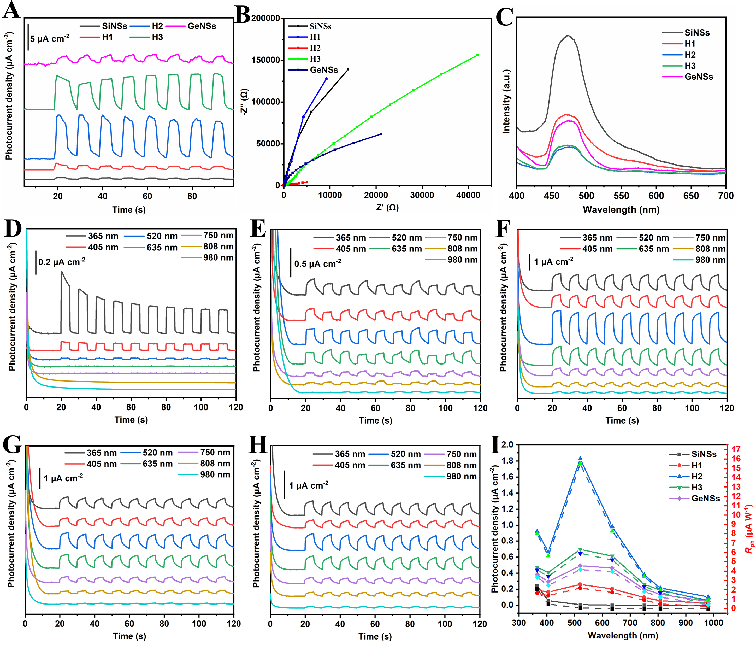
Figure 4. (A) Photoresponse behavior of SiNSs, GeNSs, and nanocomposites of H1, H2, and H3 under a 300 W xenon lamp irradiation at a bias voltage of 0.6 V; (B) Electrochemical impedance spectra (EIS) of SiNSs, GeNSs, H1, H2, and H3; (C) photoluminescence (PL) spectra of SiNSs, GeNSs, H1, H2, and H3. (D-I) Wavelength-dependent photoresponse of (D) SiNSs, (E) H1, (F) H2, (G) H3, and (H) GeNSs at Level III at a bias voltage of 0.6 V. (I) Photocurrent densities and photoresponsivities of SiNSs, H1, H2, H3, and GeNSs-PDs under various monochromatic light wavelengths at Level III under a bias potential of 0.6 V.
Photoluminescence (PL) spectra were employed to investigate the recombination and separation behaviors of photogenerated charge carriers. As depicted in Figure 4C, SiNSs exhibited strong emission arising from high recombination rates of photoexcited charge carriers. The introduction of GeNSs resulted in evident PL quenching in the GeNSs/SiNSs heterojunctions, with H2 showing the lowest PL intensity, indicating the most effective separation of electron-hole pairs and suppressed recombination due to efficient heterostructure formation.
To further investigate the photoresponse characteristics of the heterostructure nanocomposites, we used seven monochromatic light sources with wavelengths ranging from 365 to 980 nm to assess the PEC responses of SiNSs, GeNSs, and the three nanocomposites. The four different power densities for each light source are listed in Supplementary Table 1. The photoresponse of the various electrodes was first compared at a 0.6 V bias under Level III conditions. Figure 4D-I shows that SiNSs displayed apparently lower photocurrent densities compared to GeNSs and the three composites due to strong carrier recombination [Figure 4I]. At 365 nm, SiNSs exhibited a peak Pph and photoresponsivity (Rph) of 0.24 μA cm-2 and
Through comparison, we found that the Pph and Rph of the composite H1 (i.e., the mass ratio of GeNSs to SiNSs is 1:9) at different wavelengths are generally higher than those of SiNSs but lower than those of GeNSs. The Pph of H2 (mass ratio of 3:7) and H3 (mass ratio of 1:1) are pronouncedly higher than those of GeNSs and SiNSs, initially increasing and then decreasing with increasing GeNSs content in the composite. This behavior may be attributed to the insufficient heterojunction interface at low GeNSs proportions, resulting in limited improvement in photoelectric performance. As the GeNSs content increases, the enlarged heterogeneous contact interface between GeNSs and SiNSs facilitates the formation of a well-developed heterostructure, leading to a substantial increase in Pph. Under 520 nm illumination, the H2 composite exhibits the highest Pph and Rph among all samples, reaching 1.83 μA cm-2 and
The enhancement of the broad spectral response over the 365-980 nm range of the composite material by the heterostructure is consistent with the results of subsequent theoretical calculations. In addition, the detectivity of GeNSs at the maximum Pph wavelength of 520 nm (Level III) is 4.4 × 10⁷ Jones, whereas that of the H2 composite at this wavelength reaches 1.25 × 10⁸ Jones, and that of SiNSs at 520 nm is 3.16 × 10⁶ Jones. Even at 365 nm (Level III), whereas SiNSs exhibit their highest Pph, its detectivity is only 8.65 × 10⁷ Jones. This indicates that the formation of heterojunction not only enhances the Pph but also reduces the dark current. Notably, at 0 V, the responsivities of H2 at 365, 405, 520, 635, 750, 808, and 980 nm (Level III) are 1.69, 1.21, 3.75, 2.34, 0.92, 0.38, and 0.05 μA W-1, respectively, and the detectivities are 7.0 × 10⁷, 4.95 × 10⁷, 1.3 × 10⁸, 9.1 × 10⁷, 3.7 × 10⁷, 1.6 × 10⁷, 2.1 × 10⁶ Jones, respectively, demonstrating excellent self-powered broadband light detection performance (Supplementary Figure 2, under 0 V conditions, the potential difference between the working and counter electrodes arises spontaneously from electrode reactions rather than from an external power source). These performance values surpass those of reported 2D materials and heterojunctions, including GeH[12], BP[66], WS2[67], 2D Te nanosheets[68], 2D Bi[69], 2D Se[70], 2D InSe nanosheets[71], SnS2/graphene[72], and WS2-TiO2[73], as shown in Supplementary Table 2.
Under 520 nm illumination, the photoresponse test results of the H2-based PD (H2-PD) under different bias voltages [Supplementary Figure 3] show that Pph increases with increasing bias voltage, indicating that a higher bias potential can further improve the photoresponse performance of H2-PD. This is because applying a bias voltage to the working electrode induces potential differences within the material, which promote the separation of photogenerated holes and electrons and increase the carrier concentration, resulting in a marked rise in Pph with bias voltage.
The intensity of incident light notably impacts the performance of PDs. To further investigate the photoresponse behavior of the heterojunctions, we evaluated the photocurrent response of H2 at various light power densities. As illustrated in Supplementary Figure 4A and B, the Pph increases with power density under both 0.6 and 0 V bias for all tested wavelengths of illumination. Supplementary Figure 4C and D depict the relationship between Pph and optical power density (Pλ) for different wavelengths, revealing that Pph rises with increasing Pλ across all wavelengths. This suggests that the heterostructure-based self-powered PD can accurately detect light of varying intensities from ultraviolet to near-infrared wavelengths in practical applications.
In contrast to the relationship between Pph and Pλ, the Rph decreases as Pλ increases, as demonstrated in Supplementary Figure 4E and F. This decline is attributed primarily to saturation of defect states on the heterojunction's surface at higher Pλ, which increases the recombination probability of electron-hole pairs[74]. Consequently, higher Rph is achieved at lower Pλ. The Pph and Rph of H2-PD at 520 nm are markedly higher than at other wavelengths, reflecting the enhanced light absorption of the H2 heterojunction in this specific band. Under 520 nm illumination at a power density of 42.4 mW cm-2 (Level I), the maximum Rph of H2-PD was 2.9 and 28.6 μA W-1 at 0 and 0.6 V, respectively, demonstrating excellent sensitivity to green light. Additionally, H2-PD exhibited good self-powered cycling stability over 3,000 s [Supplementary Figure 5]. Interestingly, the photocurrent did not decay monotonically: it slightly increased during the initial cycles, followed by a gradual decline upon prolonged operation. This behavior arises from the competition between initial trap-state passivation (e.g., oxygen vacancies at the heterojunction interface) that temporarily enhances charge separation, and subsequent surface degradation caused by electrolyte ion adsorption and mild structural reorganization, which together limit long-term stability to 75% retention after 3,000 s.
To further examine the transport characteristics of photogenerated carriers in the GeNSs/SiNSs heterojunction, we measured the energy level structures of GeNSs and SiNSs. Figure 5A and B show the flat band (Efb) potentials vs. SCE (vs. ESCE) of GeNSs and SiNSs as -1.11 and -1.0 V, respectively, obtained through Mott-Schottky measurements with a SCE as a reference. The Efb values vs. the normal hydrogen electrode (NHE) (vs. ENHE) were calculated to be -0.87 and -0.76 V, respectively, using ENHE = ESCE + 0.2412. Typically, the flat band potential (vs. ENHE) is approximately 0.1 V more positive than the conduction band minimum (CBM) for an n-type semiconductor[75]. Accordingly, the conduction band edge positions (ECB) of GeNSs and SiNSs were -0.97 and -0.86 V, respectively. By combining these with the band gap values, the full energy band positions of GeNSs and SiNSs were obtained, as shown in
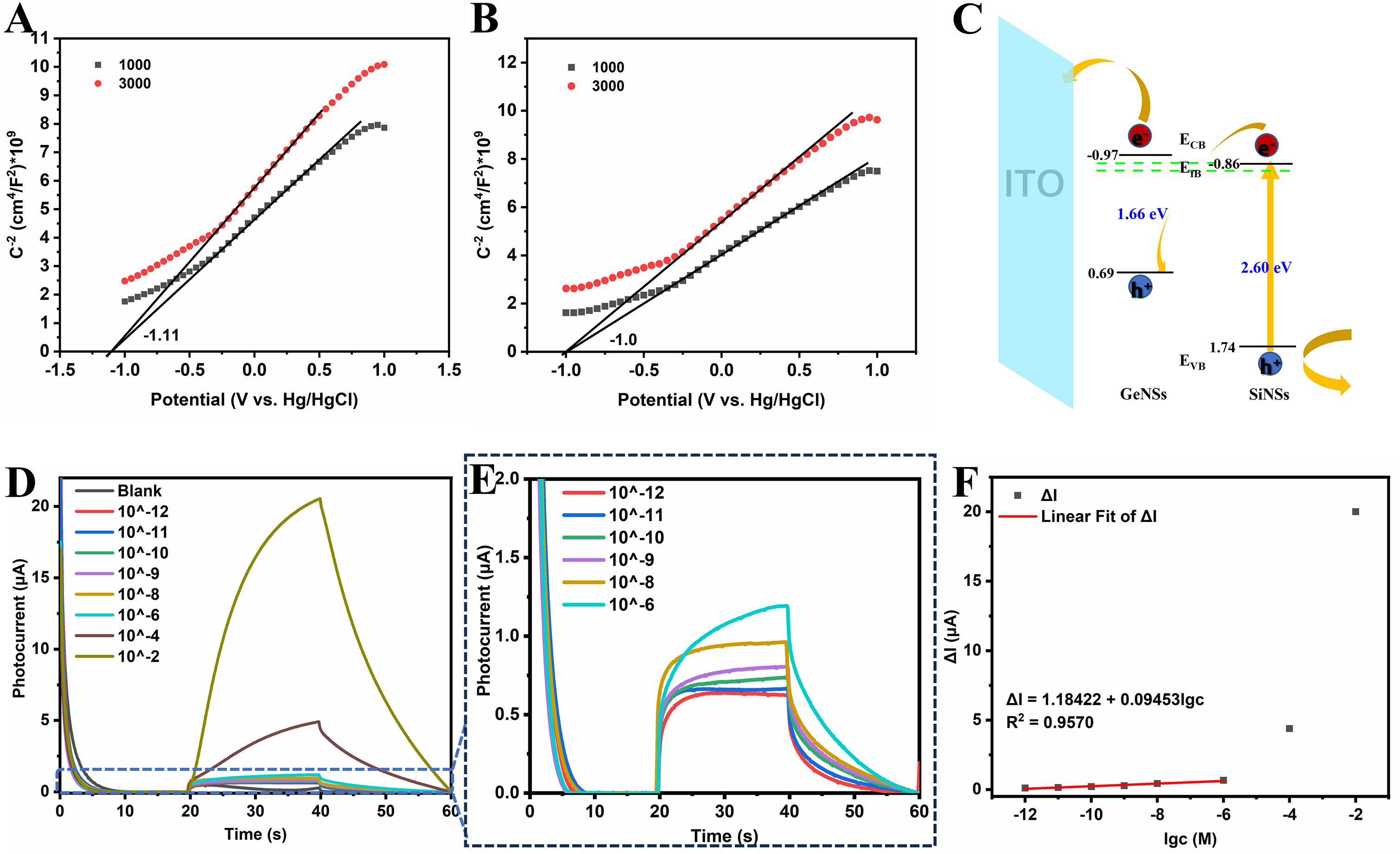
Figure 5. (A) Mott-Schottky curve of GeNSs; (B) Mott-Schottky curve of SiNSs; (C) Energy level structures of GeNSs and SiNSs. (D) Photocurrent responses of the electrode with different concentrations of tartrazine under 520 nm illumination (Level III) and a bias potential of 0.3 V. (E) Photocurrent responses of the electrode with tartrazine concentrations of 10-12, 10-11, 10-10, 10-9, 10-8, and 10-6 M. (F) A scatter plot and fitted line of photocurrent vs. log of tartrazine concentration.
Tartrazine, an azo-type acidic dye commonly used as a food additive, can pose health risks when consumed in excess. To evaluate the analytical performance of the GeNSs/SiNSs-based PEC sensor, we measured the photocurrents of the H2 electrode in various tartrazine concentrations with 0.1 M Na2SO4 as the supporting electrolyte (see the Section “EXPERIMENTAL” for detailed experimental procedures). Pulsed light irradiation was applied with a fixed period of 20 s light on followed by 20 s off; the light power density was kept constant at Level III as defined in Supplementary Table 1. As shown in Figure 5D and E, under 520 nm illumination (Level III) and a bias potential of 0.3 V, the photocurrent of H2 increased with higher tartrazine concentrations. This enhancement results from the direct oxidation of tartrazine by photogenerated holes in the valence band of SiNSs, which reduces recombination of electron-hole pairs, and allows greater accumulation of free electrons in the conduction band of GeNSs. The increase in photocurrent can then be measured as a function of tartrazine concentration. A strong linear relationship was observed between the logarithm of tartrazine concentration (10-12-10-6 M) and the photocurrent change (ΔI), described by the linear fitting equation: ΔI = 1.18422 + 0.09453lgc (R2 = 0.957) [Figure 5F]. The linear detection range spanned from 1 pM to 1 μM, with a limit of detection (LOD) estimated at 2.97 × 10⁻¹³ M (~0.3 pM). Beyond this range, at tartrazine concentrations ≥ 10-4 M, the photocurrent increase deviates from linearity due to surface saturation and Langmuir-type adsorption behavior, where the active sites on the electrode become fully occupied, altering the charge-transfer mechanism and interfacial electric field. As summarized in
The electron transfer mechanism of the GeNSs/SiNSs heterojunction was further analyzed using techniques including electron paramagnetic resonance (EPR) and in situ XPS. EPR results [Figure 6A and B] show that under illumination, both •O2- and •OH radicals exhibit evident signals in the H2 heterojunction, ruling out the type-II mechanism (under which the valence band position is insufficient to generate •OH). The Z-scheme mechanism is more consistent with the radical generation characteristics of this system: after photogenerated electrons and holes recombine at the heterointerface, they retain highly reductive electrons and highly oxidative holes, respectively, effectively driving O2 reduction and H2O oxidation processes. The peak-fitted in situ XPS spectra [Figure 6C-F] show that under illumination, the Si 2p binding energy increases while the Ge 3d binding energy decreases, indicating that photogenerated electrons flow from Si to Ge, consistent with the Z-scheme charge transfer pathway. The shift behavior of the O 1s peak is fully coordinated with the changes in the Ge 3d and Si 2p peaks. The characteristic peak of Ge-O (530.8 eV) shifts toward lower binding energy after illumination, while the characteristic peak of Si-O (532.6 eV) shifts positively, in complete agreement with the changes in electron density of GeNSs and SiNSs. The interfacial adsorbed oxygen (Oads) peak at 531.95 eV, originating from oxygen vacancies, shows only a minor change in intensity after illumination, further ruling out surface oxidation interference induced by light and demonstrating that the shifts in orbital binding energies are dominated by photogenerated carrier recombination rather than surface chemical oxidation.
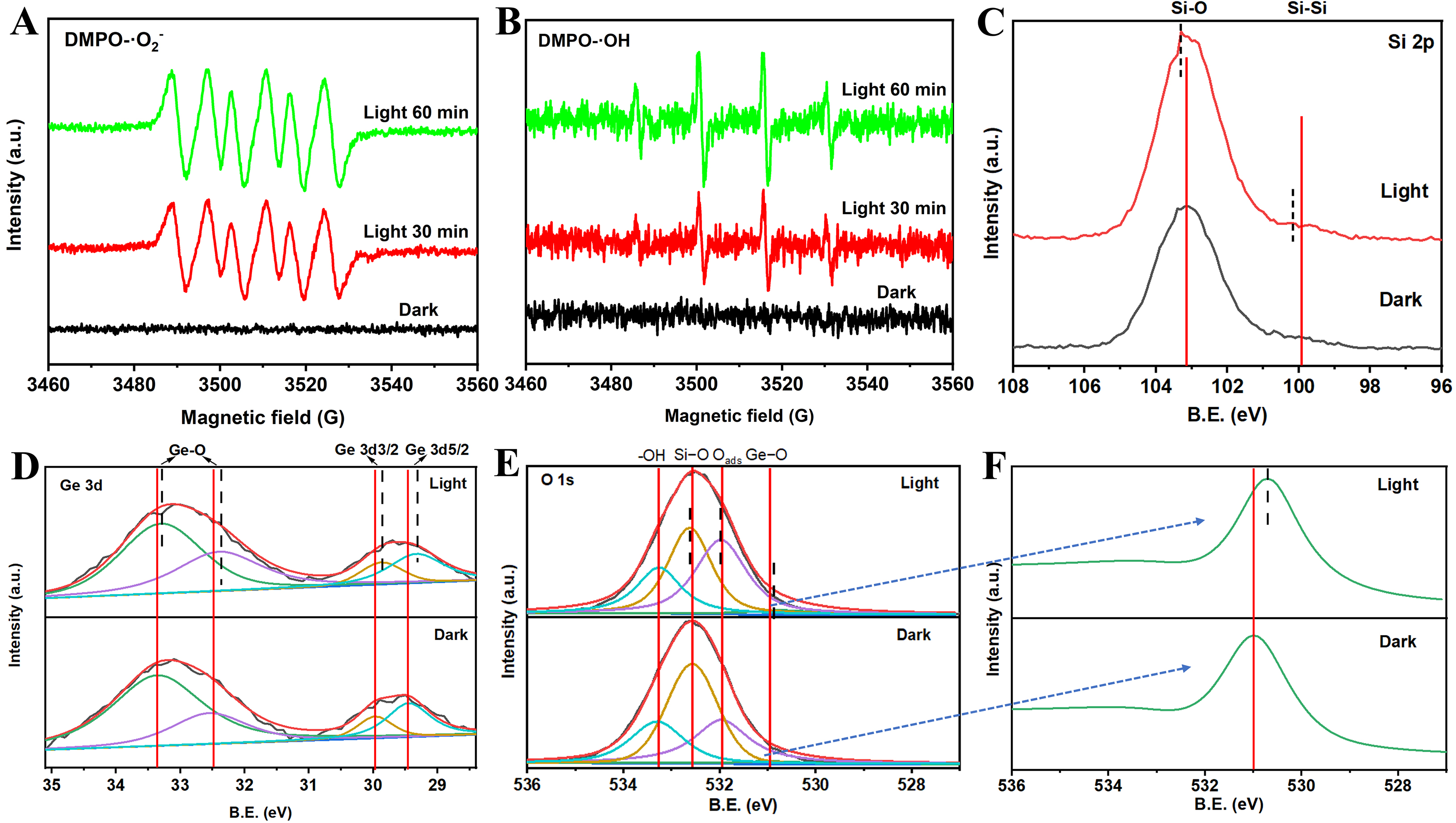
Figure 6. (A) EPR results for •O2- of H2 heterojunction under dark and Xe lamp light (30 and 60 min); (B) EPR results for •OH of H2 heterojunction under dark and light (30 and 60 min). (C-F) The in situ high-resolution XPS spectra for H2 heterojunction under dark and Xe lamp light: (C) Si 2p, (D) Ge 3d, (E) O 1s. (F) Partial enlarged view of (E).
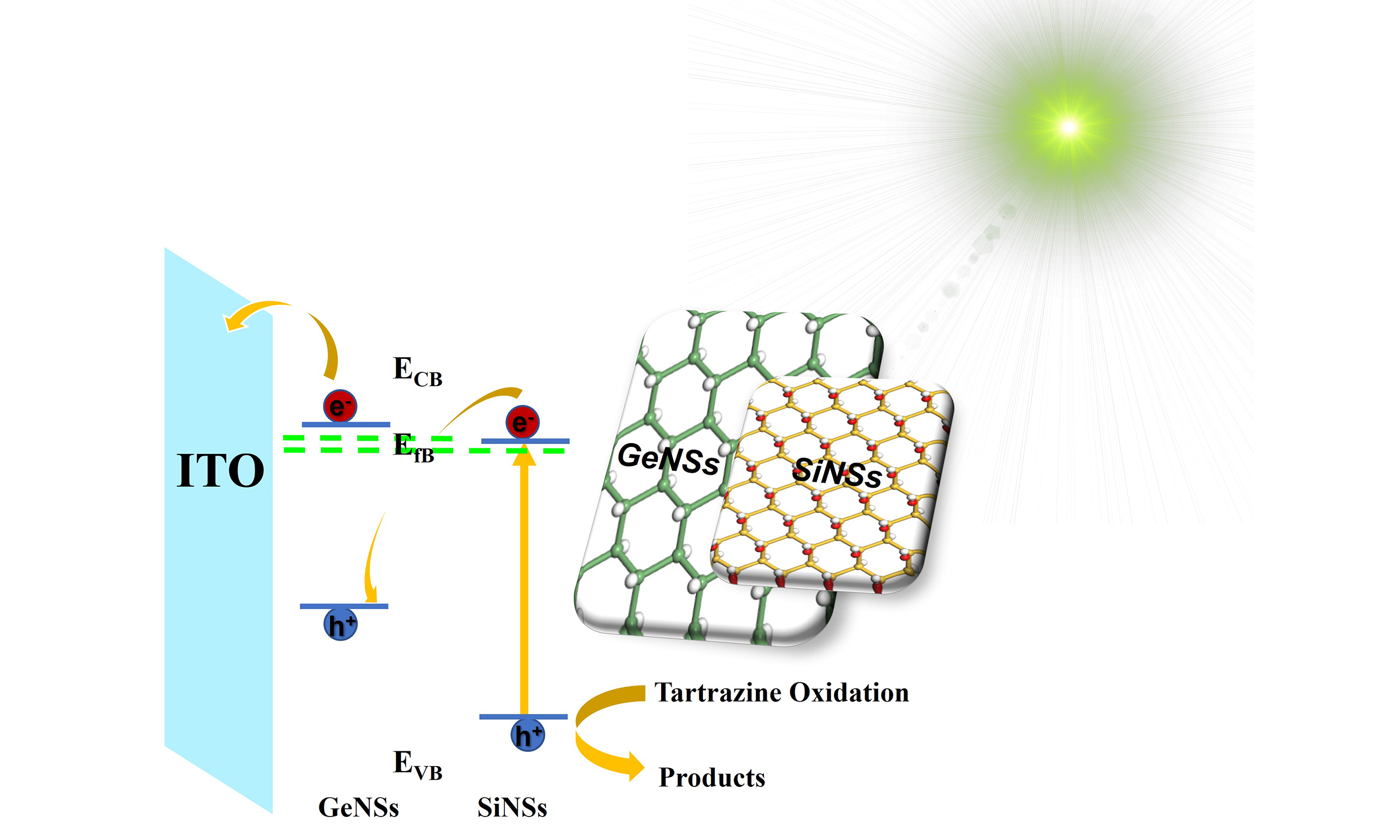
Combining the above EPR and in situ XPS evidence, the PEC sensing mechanism of the GeNSs/SiNSs heterojunction for tartrazine detection is schematically illustrated in Figure 7A and can be described as follows. In this Z-scheme heterojunction system, upon light irradiation, the photogenerated electrons in the conduction band of SiNSs recombine with the photogenerated holes in the valence band of GeNSs through the heterointerface, leaving highly reductive electrons in the conduction band of GeNSs and highly oxidative holes in the valence band of SiNSs. The EPR results confirm the coexistence of •O2- and •OH radicals, which is characteristic of the Z-scheme mechanism rather than the type-II mechanism. When the target molecule tartrazine (an electron donor) is present in solution, it is preferentially oxidized by the strongly oxidizing holes accumulated in the valence band of SiNSs. This process effectively suppresses the recombination of photogenerated carriers, leading to an increased electron density in the conduction band of GeNSs, which macroscopically manifests as a marked increase in photocurrent. The photocurrent increment (ΔI) exhibits a good linear relationship with the tartrazine concentration in the range of 1 pM to 1 μM, enabling highly sensitive detection of tartrazine.
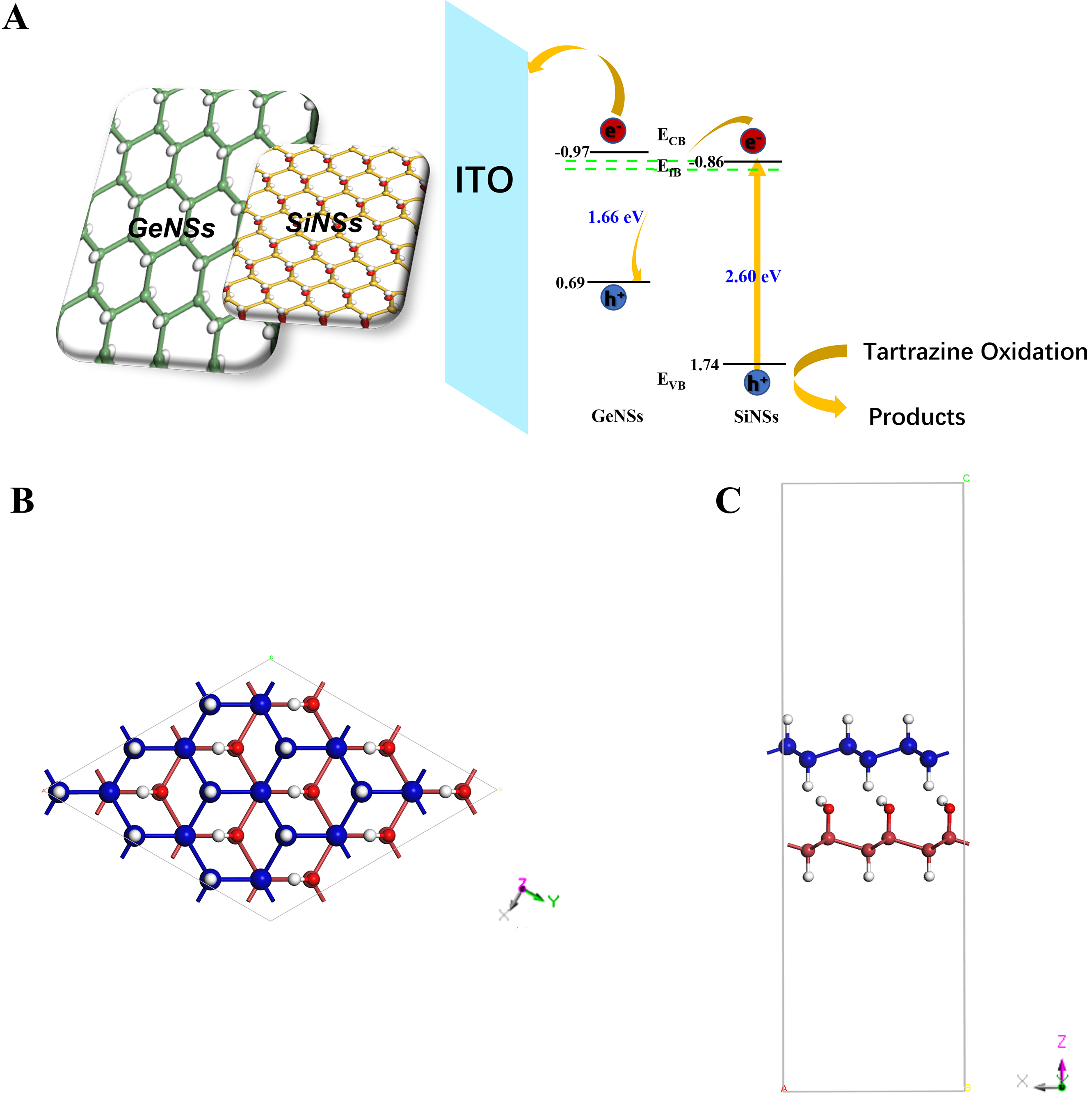
Figure 7. (A) Schematic diagram of the energy level structure of GeNSs/SiNSs Z-scheme heterojunction and the mechanism of detecting tartrazine. (B and C) The structure of germanane/siloxene heterostructure with clearly labeled x-, y-, and z-axes: (B) Top view, (C) Side view.
THEORETICAL ANALYSIS
To gain a deeper understanding of the electron transfer mechanisms in GeNSs/SiNSs heterojunctions, we simulated a van der Waals (vdW) heterostructure by constructing a thermodynamically favorable structure of a germanane/siloxene heterobilayer, where the germanane and siloxene frameworks are stacked in an AB stacking[78,79], as shown in Figure 7B and C. To determine the most stable stacking structure of the heterobilayer, we systematically calculated the binding energy of the heterostructure with interlayer distances ranging from 3.0 to 7.0 Å. The calculation results confirm that the heterobilayer achieves the lowest binding energy and optimal thermodynamic stability at an interlayer distance of 5.3 Å [Figure 8A]. This heterostructure is a direct bandgap semiconductor, similar to the germanane and siloxene monolayers, but has a smaller bandgap (1.898 eV) than those of the individual monolayers
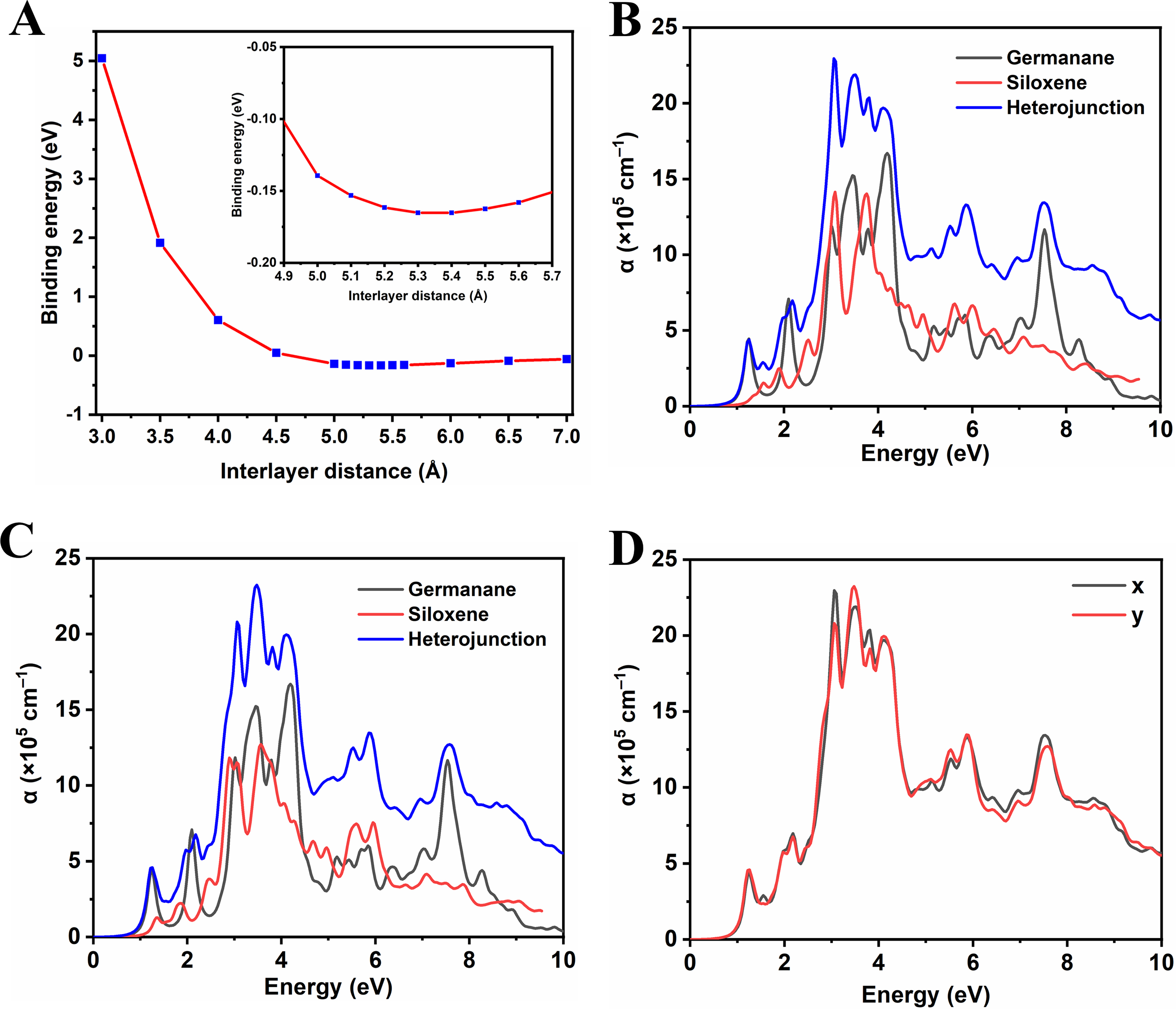
Figure 8. The optical properties of the germanane/siloxene heterostructure. (A) Calculated energy curve of germanane/siloxene as a function of interlayer distance. (B and C) represent the optical absorption coefficient α of the isolated germanane and siloxene layers and the germanane/siloxene heterostructure in the x and y directions, respectively. (D) Comparison of the optical absorption coefficient α of germanane/siloxene in the x and y directions.
The calculations of optical properties indicate slight differences in the light absorption coefficients of the siloxene monolayer and the heterostructure in the x and y directions [Figure 8B and C]. However, the light absorption coefficient curves for the bilayer heterojunction in the x and y directions nearly overlap
CONCLUSIONS
In conclusion, we successfully constructed direct Z-scheme 2D-2D GeNSs/SiNSs heterojunctions for the first time, which demonstrate potential for self-powered, broadband-response, and high-sensitivity PEC PDs. The formation of these direct Z-scheme heterojunctions substantially enhances the separation of photogenerated electrons and holes, thereby improving the redox capability of the composite materials and consequently boosting the photocurrent response. Furthermore, the heterojunctions effectively extend the light absorption range of SiNSs, enabling a broader spectrum of light detection. The optimal mass ratio of GeNSs to SiNSs was determined to be 3:7, which yielded superior performance compared with pure GeNSs and SiNSs. Notably, the PEC PD based on the GeNSs/SiNSs heterojunction exhibited the strongest light response at 520 nm and also demonstrated its capability as a PEC sensor for detecting the common azo food additive tartrazine. This sensor showcased a wide linear detection range for tartrazine concentration along with an ultra-low detection limit, underscoring the considerable application potential of GeNSs/SiNSs heterojunctions in high-sensitivity and low-detection-limit PEC sensors. Although the present data were collected from three representative mass ratios, we acknowledge that a more detailed compositional series would be necessary to pinpoint the exact optimum. Future work could combine systematic TEM-EDS mapping and local photocurrent measurements to directly correlate the spatial distribution of GeNSs and SiNSs with the photoresponse at the nanoscale, thereby providing direct experimental verification of the optimal distribution and the role of heterointerface density.
DECLARATIONS
Acknowledgments
The authors would like to thank Shiyanjia Lab (www.shiyanjia.com) for the Raman spectroscopy, XPS and EPR measurements, and thank Ceshigo for the DFT calculations. In addition, the authors would like to thank Bo Song from SCI-GO (www.sci-go.com) for the SEM and in situ XPS measurements.
Authors’ contributions
Conception and design of the work: Zhao, F.
Data acquisition and analysis: Liu, R.; Chen, H.
Writing - original draft, data interpretation: Zhao, F.; Liu, R.; Chen, H.
Investigation: Yuan, W.; Fu, H.
Writing - review and editing: Zhao, F.; Feng, Y.
Availability of data and materials
The data supporting the findings of this study are available within this Article and its Supplementary Materials. Further data are available from the corresponding authors upon request.
AI and AI-assisted tools statement
Not applicable.
Financial support and sponsorship
This work was supported by the Taishan Scholar Project of Shandong Province of China (Grant No. tsqn202312187), the Natural Science Foundation of Shandong Province (ZR2024QE220), and the National Natural Science Foundation of China (Grant No. 52103093).
Conflicts of interest
Zhao, F. is affiliated with Shandong Chambroad Holding Group Co., Ltd., The other authors declared that there are no conflicts of interest.
Ethical approval and consent to participate
Not applicable.
Consent for publication
Not applicable.
Copyright
© The Author(s) 2026.
Supplementary Materials
REFERENCES
1. Li, X.; Wang, S.; Bi, Y.; Shen, Z.; Han, J.; Li, H. Recent advances in 2D nanomaterials as photocatalysts for sustainable CO2 reduction. Chem. Eng. J. 2026, 542, 178146.
2. Tang, J.; Guo, C.; Wang, T.; et al. A review of g-C3N4-based photocatalytic materials for photocatalytic CO2 reduction. Carbon. Neutral. 2024, 3, 557-83.
3. Yang, Z.; Ji, Y.; Ren, J.; Wang, X.; Xue, Y.; Tian, J. 2D/2D heterointerface engineering of Ni2P/ZnIn2S4 photocatalysts for enhanced photocatalytic H2 evolution. Mater. Rep. Energy. 2026, 6, 100401.
4. Wu, R.; He, C.; Meng, X.; et al. Competition between phonon-assisted and exciton photoluminescence modulated by temperature in WSe2/graphene nanosheet heterostructures for flexible optoelectronic sensor devices. ACS. Appl. Nano. Mater. 2024, 7, 16941-8.
5. Chen, J.; Bailey, C. S.; Cui, D.; et al. Stacking independence and resonant interlayer excitation of monolayer WSe2/MoSe2 heterostructures for photocatalytic energy conversion. ACS. Appl. Nano. Mater. 2020, 3, 1175-81.
6. Zhao, F.; Feng, Y.; Feng, W. Germanium-based monoelemental and binary two-dimensional materials: theoretical and experimental investigations and promising applications. InfoMat 2022, 4, e12365.
7. Nakano, H.; Ishii, M.; Nakamura, H. Preparation and structure of novel siloxene nanosheets. Chem. Commun. 2005, 23, 2945-7.
8. Bianco, E.; Butler, S.; Jiang, S.; Restrepo, O. D.; Windl, W.; Goldberger, J. E. Stability and exfoliation of germanane: a germanium graphane analogue. ACS. Nano. 2013, 7, 4414-21.
9. Jiang, S.; Arguilla, M. Q.; Cultrara, N. D.; Goldberger, J. E. Covalently-controlled properties by design in group IV graphane analogues. Acc. Chem. Res. 2014, 48, 144-51.
10. Xiao, M.; Yin, X.; Song, H.; Lv, Y.; Xiao, B. Tunable band gaps and high carrier mobilities in germanene by Si doping in the presence of an external electric field: field effect transistors. Phys. B. Condens. Matter. 2024, 682, 415859.
11. Madhushankar, B. N.; Kaverzin, A.; Giousis, T.; et al. Electronic properties of germanane field-effect transistors. 2D. Mater. 2017, 4, 021009.
12. Liu, N.; Qiao, H.; Xu, K.; et al. Hydrogen terminated germanene for a robust self-powered flexible photoelectrochemical photodetector. Small 2020, 16, 2000283.
13. Roy, P. K.; Hartman, T.; Šturala, J.; Luxa, J.; Melle-Franco, M.; Sofer, Z. Hydrogen-terminated two-dimensional germanane/silicane alloys as self-powered photodetectors and sensors. ACS. Appl. Mater. Interfaces. 2023, 15, 25693-703.
14. Zhang, Q.; Ziad, M.; Liu, Z.; Li, H.; Fu, A. Germanene/MoS2 heterostructure as promising anchoring and electrocatalyzing material for high performance lithium-sulfur batteries: a computational study. J. Energy. Storage. 2025, 109, 115205.
15. Wu, B.; Šturala, J.; Veselý, M.; et al. Functionalized germanane/SWCNT hybrid films as flexible anodes for lithium-ion batteries. Nanoscale. Adv. 2021, 3, 4440-6.
16. Zhang, X.; Xin, L.; Murugesan, K.; et al. Two-dimensional siloxene: a promising silicon-based material with enhanced volume stability for Li-ion battery anode. Chem. Eng. J. 2026, 532, 174513.
17. Guo, Q.; Han, Y.; Chen, N.; Qu, L. Few-layer siloxene as an electrode for superior high-rate zinc ion hybrid capacitors. ACS. Energy. Lett. 2021, 6, 1786-94.
18. Zhang, E.; Xie, D.; Hong, Y.; et al. Siloxene coupled graphene anode membrane with Zn-ion intercalation for all-solid-state Zn-ion hybrid supercapacitors. Chem. Eng. J. 2025, 523, 168578.
19. Huang, Y.; Xiao, S.; Zhong, Z.; et al. A novel ratiometric biosensor based on germanene nanosheets for rapid and sensitive BRCA1 detection in differentiating T cells. Biosens. Bioelectron. 2026, 298, 118411.
20. Song, Z.; Ang, W. L.; Sturala, J.; et al. Functionalized germanene-based nanomaterials for the detection of single nucleotide polymorphism. ACS. Appl. Nano. Mater. 2021, 4, 5164-75.
21. Kovalska, E.; Antonatos, N.; Luxa, J.; Sofer, Z. Edge-hydrogenated germanene by electrochemical decalcification-exfoliation of CaGe2: germanene-enabled vapor sensor. ACS. Nano. 2021, 15, 16709-18.
22. Ramachandran, R.; Leng, X.; Zhao, C.; Xu, Z.; Wang, F. 2D siloxene sheets: a novel electrochemical sensor for selective dopamine detection. Appl. Mater. Today. 2020, 18, 100477.
23. Rosli, N. F.; Rohaizad, N.; Sturala, J.; Fisher, A. C.; Webster, R. D.; Pumera, M. Siloxene, germanane, and methylgermanane: functionalized 2D materials of group 14 for electrochemical applications. Adv. Funct. Mater. 2020, 30, 1910186.
24. Giousis, T.; Fang, S.; Miola, M.; et al. Germanane and butyl-functionalized germanane as visible-light photocatalysts for the degradation of water pollutants. J. Environ. Chem. Eng. 2023, 11, 109784.
25. Li, S.; Wang, H.; Li, D.; et al. Siloxene nanosheets: a metal-free semiconductor for water splitting. J. Mater. Chem. A. 2016, 4, 15841-4.
26. Ng, S.; Sturala, J.; Vyskocil, J.; et al. Two-dimensional functionalized germananes as photoelectrocatalysts. ACS. Nano. 2021, 15, 11681-93.
27. Zhao, F.; Feng, Y.; Wang, Y.; et al. Two-dimensional gersiloxenes with tunable bandgap for photocatalytic H2 evolution and CO2 photoreduction to CO. Nat. Commun. 2020, 11, 1443.
28. Li, M.; Ramachandran, R.; Sakthivel, T.; Wang, F.; Xu, Z. Siloxene: an advanced metal-free catalyst for efficient photocatalytic reduction of aqueous Cr(VI) under visible light. Chem. Eng. J. 2021, 421, 129728.
29. Imagawa, H.; Wu, X.; Itahara, H.; et al. Photocatalytic NO removal over calcium-bridged siloxenes under ultraviolet and visible light irradiation. Dalton. Trans. 2018, 47, 7070-6.
30. Luo, J.; Selopal, G. S.; Tong, X.; Wang, Z. Colloidal quantum dots and two-dimensional material heterostructures for photodetector applications. Electron 2024, 2, e30.
31. Xiao, J.; Xiong, X.; Shi, X.; et al. High-performance edge-contact monolayer molybdenum disulfide transistors. Research 2025, 8, 0593.
32. Qiu, D.; Gong, C.; Wang, S.; et al. Recent advances in 2D superconductors. Adv. Mater. 2021, 33, 2006124.
33. Wang, Y.; Zhao, F.; Wang, Y.; et al. Broadband self-powered photoelectrochemical photodetector based on Te/Se heterostructure nanocomposites. Compos. Commun. 2022, 32, 101175.
34. Li, P.; Deng, D.; Liu, Y.; et al. Unveiling the defect-accelerated charge transfer mechanism in ZnIn2S4/g-C3N4 Z-scheme heterojunctions for efficient solar fuel production. Carbon. Neutral. 2026, 5, e70139.
35. Tan, X.; Loh, J. Y.; Mohamed, A. R.; Ong, W. Two-in-one redox photocatalysis: cooperative hydrogen evolution and benzaldehyde production via 2D MoS2 cocatalyst-loaded hydrangea-like Zn3In2S6. Mater. Rep. Energy. 2025, 5, 100374.
36. Lee, J.; Kim, Y.; Kwak, B. S.; et al. Atomic-scale structurally locked 1T/2H-MoS2/ZnS Z-scheme heterojunctions for prolonged charge kinetics and dual-functional photocatalysis. Energy. Environ. Mater. 2026, e70493.
37. Yu, H.; Wu, X. Ripples in two-dimensional transition metal sulfides: formation mechanism, optoelectronic regulation, and application prospects. Battery. Energy. 2026, 5, e70108.
38. Ding, G.; Wang, Z.; Zhang, J.; Wang, P.; Chen, L.; Liao, G. Layered double hydroxides-based Z-scheme heterojunction for photocatalysis. EcoEnergy 2024, 2, 22-44.
39. Yuan, M.; Jiang, L.; Mao, S.; Zhou, W.; Lin, X.; Yuan, Y. Construction Z-scheme heterostructure by WO3 nanocubes embedded g-C3N4 nanosheets with n-π* electronic transition for enhanced visible light driven photocatalysis. J. Photochem. Photobiol. A. Chem. 2025, 469, 116581.
40. Zhu, Q.; Sun, J.; Zhu, Y.; Jiang, H.; Yan, W.; Shen, J. In situ phase transition and Cu doping synergistically regulate perovskite Z-scheme heterojunction for photocatalytic CO2 reduction. Energy. Environ. Mater. 2026, e70387.
41. Mandari, K. K.; Kang, M. g-C3N4/MXene-based heterostructures: advanced catalysts for efficient and sustainable renewable energy production. Adv. Ind. Eng. Chem. 2025, 1, 14.
42. Wang, S.; Hao, W.; Liu, Z.; Niu, X.; Wang, L.; Zhao, Q. Two-dimensional direct Z-scheme heterojunction photocatalysts for highly efficient energy conversion and chemical synthesis. ACS. Nano. 2025, 20, 137-62.
43. Li, Y.; Wang, J. 2D/2DZ-scheme WO3/g-C3N4 heterojunctions for photocatalytic organic pollutant degradation and nitrogen fixation. Mater. Adv. 2024, 5, 749-61.
44. Tuc Altaf, C.; Yaman, E.; Karagoz, E.; Colak, Colak.; Demirci Sankir, E.; Sankir, M. Self-powered photoelectrochemical photodetectors based on a CsPbBr3/S-g-C3N4 heterojunction-sensitized 3D ZnO nanostructured thin film. ACS. Appl. Nano. Mater. 2024, 7, 8186-96.
45. Xiao, W.; Xu, W.; Huang, W.; et al. Bismuth-based BiO BrxI1-x/Ti3C2 MXene schottky nanocomposites for Hg2+ photoelectrochemical sensors. ACS. Appl. Nano. Mater. 2022, 5, 18168-77.
46. Qu, J.; Cheng, H.; Lan, H.; et al. Space-confined growth of ultrathin P-type GeTe nanosheets for broadband photodetectors. Small 2024, 20, 2309391.
47. Yang, W.; Chen, T.; Xie, L.; Yu, Y.; Long, M.; Xu, L. A systematic study of switching, optoelectronics, and gas-sensitive properties of PCF-graphene-based nanodevices: insights from DFT study. Carbon. Neutral. 2024, 3, 904-17.
48. Zeng, W.; Zhang, Y.; Wu, Z.; et al. Hierarchically converged defect engineering with 2-dimensional black phosphorus/MXene sequence for sensitive photoelectrochemical-electrostatic sensors. Research 2025, 8, 0966.
49. Qin, J.; Tang, Y.; Zeng, Y.; Liu, X.; Tang, D. Recent advances in flexible sensors: from sensing materials to detection modes. TrAC. Trends. Anal. Chem. 2024, 181, 118027.
50. Awasthi, T.; Kaur, S.; Joshi, S.; Kaur, R. Advances in smart indicators and their integration with sensor systems for foodborne hazard monitoring. Food. Control. 2026, 183, 111932.
51. Bhardwaj, S. K.; Deep, A.; Bhardwaj, N.; Wangoo, N. Recent advancements in nanomaterial based optical detection of food additives: a review. Analyst 2023, 148, 5322-39.
52. Han, J.; Fu, Z.; Wei, J.; et al. 2D materials-based next-generation multidimensional photodetectors. Light. Sci. Appl. 2025, 14, 362.
53. Qiu, Z.; Tang, D. Nanostructure-based photoelectrochemical sensing platforms for biomedical applications. J. Mater. Chem. B. 2020, 8, 2541-61.
54. Ali, M. A.; Tchalala, M. R. Chemical synthesis of silicon nanosheets from layered calcium disilicide. J. Phys. Conf. Ser. 2014, 491, 012009.
55. Hui, X.; Li, L.; Xia, Q.; et al. Interface engineered Sb2O3/W18O49 heterostructure for enhanced visible-light-driven photocatalytic N2 reduction. Chem. Eng. J. 2022, 438, 135485.
56. Jiang, H.; Zhu, X.; Wang, D.; et al. Tunable type-I band alignment and electronic structure of GaSe/MoSi2N4 van der Waals heterostructure. Microstructures 2025, 5, 2025009.
57. Sturala, J.; Luxa, J.; Matějková, S.; et al. Exfoliation of Calcium germanide by alkyl halides. Chem. Mater. 2019, 31, 10126-34.
58. Liu, N.; Xu, K.; Lei, Y.; et al. Germanene nanosheets: achieving superior sodium-ion storage via pseudointercalation reactions. Small. Struct. 2021, 2, 2100041.
59. Chang, C.; Yang, H.; Mu, W.; et al. In situ fabrication of bismuth oxyiodide (Bi7O9I3/Bi5O7I) n-n heterojunction for enhanced degradation of triclosan (TCS) under simulated solar light irradiation. Appl. Catal. B. Environ. 2019, 254, 647-58.
60. Hu, K.; Tian, J.; Zhou, Z.; Zhao, D.; Guan, X. Direct Z-scheme photocatalytic systems based on vdW heterostructures for water splitting and CO2 reduction: fundamentals and recent advances. Microstructures 2024, 4, 2024021.
61. Kong, X. Y.; Choo, Y. Y.; Chai, S.; Soh, A. K.; Mohamed, A. R. Oxygen vacancy induced Bi2WO6 for the realization of photocatalytic CO2 reduction over the full solar spectrum: from the UV to the NIR region. Chem. Commun. 2016, 52, 14242-5.
62. Lu, Y.; Chen, M.; Huang, T.; et al. Oxygen vacancy-dependent photocatalytic activity of well-defined Bi2Sn2O7-x hollow nanocubes for NOx removal. Environ. Sci. Nano. 2021, 8, 1927-33.
63. Ni, H.; Li, M.; Hu, Y.; et al. Two-dimensional SnSe/GeSe van der Waals heterostructure with strain-tunable electronic and optical properties. J. Phys. Chem. Solids. 2019, 131, 223-9.
64. Ma, J.; Xu, L.; Yin, Z.; et al. “One stone four birds” design atom co-sharing BiOBr/Bi2S3 S-scheme heterojunction photothermal synergistic enhanced full-spectrum photocatalytic activity. Appl. Catal. B. Environ. Energy. 2024, 344, 123601.
65. Cultrara, N. D.; Wang, Y.; Arguilla, M. Q.; et al. Synthesis of 1T, 2H, and 6R germanane polytypes. Chem. Mater. 2018, 30, 1335-43.
66. Ren, X.; Li, Z.; Huang, Z.; et al. Environmentally robust black phosphorus nanosheets in solution: application for self-powered photodetector. Adv. Funct. Mater. 2017, 27, 1606834.
67. Wang, B.; Zhu, W.; Tang, P.; Qi, X. Graphene-like tungsten sulphide nanosheets prepared by hydrothermal intercalation/exfoliation route and its application for photodetector. Fullerenes. Nanotubes. Carbon. Nanostruct. 2019, 27, 928-33.
68. Xie, Z.; Xing, C.; Huang, W.; et al. Ultrathin 2D nonlayered tellurium nanosheets: facile liquid-phase exfoliation, characterization, and photoresponse with high performance and enhanced stability. Adv. Funct. Mater. 2018, 28, 1705833.
69. Huang, H.; Ren, X.; Li, Z.; et al. Two-dimensional bismuth nanosheets as prospective photo-detector with tunable optoelectronic performance. Nanotechnology 2018, 29, 235201.
70. Fan, T.; Xie, Z.; Huang, W.; Li, Z.; Zhang, H. Two-dimensional non-layered selenium nanoflakes: facile fabrications and applications for self-powered photo-detector. Nanotechnology 2019, 30, 114002.
71. Li, Z.; Qiao, H.; Guo, Z.; et al. High-performance photo-electrochemical photodetector based on liquid-exfoliated few-layered InSe nanosheets with enhanced stability. Adv. Funct. Mater. 2017, 28, 1705237.
72. Qiao, H.; Chen, X.; Wang, B.; Huang, Z.; Qi, X. Novel tin disulfide/graphene photoelectrochemical photodetector based on solid-state electrolytes and its performances. J. Mater. Sci. Mater. Electron. 2019, 30, 3208-13.
73. Ren, X.; Qiao, H.; Huang, Z.; et al. Investigating the photocurrent generation and optoelectronic responsivity of WS2-TiO2 heterostructure. Opt. Commun. 2018, 406, 118-23.
74. Lan, C.; Li, C.; Yin, Y.; Guo, H.; Wang, S. Synthesis of single-crystalline GeS nanoribbons for high sensitivity visible-light photodetectors. J. Mater. Chem. C. 2015, 3, 8074-9.
75. Li, Y.; Sun, B.; Lin, H.; et al. Efficient visible-light induced H2 evolution from T-CdxZn1-xS/defective MoS2 nano-hybrid with both bulk twinning homojunctions and interfacial heterostructures. Appl. Catal. B. Environ. 2020, 267, 118702.
76. Li, X.; Wan, Y.; Deng, F.; et al. Advances in Z-scheme and S-scheme heterojunctions for photocatalytic and photoelectrocatalytic H2O2 production. Chin. Chem. Lett. 2025, 36, 111418.
77. Chen, X.; Wu, W.; Zhang, Q.; et al. Z-scheme Bi2O3/CuBi2O4 heterojunction enabled sensitive photoelectrochemical detection of aflatoxin B1 for health care, the environment, and food. Biosens. Bioelectron. 2022, 214, 114523.
78. Jin, H.; Dai, Y.; Ma, X.; Yu, L.; Wei, W.; Huang, B. Enhancement of photocatalytic activity of a two-dimensional GeH/graphene heterobilayer under visible light. RSC. Adv. 2015, 5, 52264-8.
Cite This Article
 Open Access
How to Cite
Liu, R.; Chen, H.; Yuan, W.; Fu, H.; Zhao, F.; Feng, Y. Direct Z-scheme siloxene germanane nanosheet heterojunctions for broadband photodetection and ultrasensitive photoelectrochemical sensing. Microstructures 2026, 6, 20260123. https://dx.doi.org/10.20517/microstructures.2026.57
Download Citation
If you have the appropriate software installed, you can download article citation data to the citation manager of your choice. Simply select your manager software from the list below and click on download.
Export Citation File
Type of Import
Tips on Downloading Citation
Citation Manager File Format
Type of Import
Direct Import: When the Direct Import option is selected (the default state), a dialogue box will give you the option to Save or Open the downloaded citation data. Choosing Open will either launch your citation manager or give you a choice of applications with which to use the metadata. The Save option saves the file locally for later use.
Indirect Import: When the Indirect Import option is selected, the metadata is displayed and may be copied and pasted as needed.
About This Article
Copyright

Data & Comments
Data
0











Comments
Comments must be written in English. Spam, offensive content, impersonation, and private information will not be permitted. If any comment is reported and identified as inappropriate content by OAE staff, the comment will be removed without notice. If you have any queries or need any help, please contact us at [email protected].