


Progress in atomic layer deposition of metal oxides for efficient and stable perovskite solar cells
 0
0 
Abstract
Perovskite solar cells (PSCs) are widely recognized as one of the most promising candidates for next-generation photovoltaics (PV), attributed to their outstanding power conversion efficiency and easily adjustable bandgap. Nevertheless, their practical commercialization remains challenging due to inherent material instabilities and rapid degradation triggered by exposure to moisture, oxygen, ultraviolet light, and thermal stress. In response, atomic layer deposition (ALD) has gained prominence as an advanced thin-film deposition technique, offering atomic-level precision and enabling the fabrication of uniform, conformal, and defect-minimized metal oxide (MO) layers. The ALD MOs serve versatile roles as charge transport layers, interfacial passivation coatings, and encapsulation barriers, collectively enhancing device performance, mechanical integrity, and operational durability. This review highlights the working mechanism of ALD, structural features of PSCs, and key strategies that leverage ALD-grown MOs to address efficiency loss and instability issues. Specific focus is given to defect passivation and protection against environmental factors. Moreover, challenges including precursor optimization, process compatibility with PSC architectures, and cost considerations are examined, along with future perspectives for industrial translation. Finally, the integration of ALD MOs holds strong potential to deliver the stability, efficiency, and scalability essential for the industrial application of PSCs in sustainable PV technologies.
Keywords
INTRODUCTION
Global industrialization powered by fossil fuels has driven significant economic growth, yet the resulting greenhouse-gas emissions have accelerated climate change. In response, international initiatives such as the Paris Agreement have emphasized carbon neutrality and stimulated a broad shift toward renewable and low-carbon energy systems[1-3]. Among various sustainable technologies, solar energy has gained particular importance due to its abundance and scalability. Photovoltaics (PVs) that convert sunlight directly into electricity represent a central component of this transition[4,5].
Crystalline silicon (c-Si) solar cells currently dominate the PV market due to their high efficiency and long-term reliability. Owing to decades of accumulated research and development, Si PVs have achieved both high power conversion efficiency (PCE) and long-term reliability, with stable efficiencies exceeding 20% in practice[6,7]. However, their indirect bandgap, high-temperature wafer processing, and mechanical rigidity limit further cost reduction and hinder applications in emerging flexible or lightweight devices[8].
A wide range of inorganic and organic materials have been investigated. Thin-film solar cells such as CIGS (Cu(In,Ga)Se2), CdTe, and CZTS (Cu2ZnSnS4) initially attracted significant attention due to their excellent light-absorbing properties and relatively simple fabrication processes[9-13]. However, challenges including reliance on scarce elements, toxicity, and limited long-term stability have hindered their large-scale commercialization[14]. Organic and polymer-based solar cells, on the other hand, offer the advantages of low-cost and low-temperature solution processing, yet their inherently limited charge-transport properties and modest optoelectronic performance have prevented them from matching the competitiveness of silicon photovoltaics[15-18].
Organic-inorganic halide perovskites first reported by Miyasaka’s group in 2009 have emerged as a highly promising class of next-generation photoabsorber materials, demonstrating remarkable progress over the past decade[19-21]. Perovskite solar cells (PSCs) combine several unique advantages not typically offered by conventional semiconductors, including a strong optical absorption coefficient, long charge diffusion lengths, bandgap tuning via compositional engineering, and intrinsic defect tolerance[22-24]. Since the initial report, in which a PCE of 3.9% was achieved, PSCs have rapidly advanced to exceed 27% within just over a decade, approaching and even surpassing the performance of c-Si[25,26]. The facile bandgap tunability of halide perovskites further enables integration into tandem architectures with Si solar cells, while low-cost solution-based processing allows scalable large-area fabrication[27-30]. Owing to these attributes, PSCs are now recognized in academic research as one of the leading candidates for next-generation photovoltaic technologies.
However, the most critical obstacle hindering the commercialization of PSCs lies in instability. Composed of weak ionic bonds, the perovskite crystal lattice is inherently fragile, and readily undergoes degradation when exposed to moisture, oxygen, ultraviolet (UV) radiation, and thermal stress[31-35]. In particular, moisture disrupts the ionic bonding within the lattice, leading to irreversible structural collapse, while oxygen and UV light trigger photocatalytic oxidation reactions that interfere with charge transport pathways[36,37]. As a result, maintaining reliable performance over extended periods remains highly challenging. Besides, solution based thin-film fabrication techniques such as spin coating are highly sensitive to external parameters including humidity, temperature, and solvent evaporation rate, making it difficult to achieve uniformity and reproducibility[38-41]. Unavoidably, the microscopic pinholes and defects are introduced, thereby performance losses become more pronounced as device areas scale up. Although various mitigation strategies such as interface engineering and additive incorporation have been explored, fundamental limitations still persist[42-45].
To overcome the limitations of solution-based processes, vacuum deposition techniques have been explored as alternative routes for thin-film fabrication[46]. High-quality film deposition is facilitated in a vacuum environment, where the attenuation of impurity concentrations and the exclusion of external contaminants are achieved. Accordingly, vacuum deposition techniques such as electron-beam evaporation (EBE), thermal evaporation (TE), and chemical vapor deposition (CVD) have already been applied to PSC fabrication with notable success[47-50]. Nevertheless, challenges remain for film quality and large-scale commercialization due to the high cost of equipment, complex process control requirements, and the limited availability of suitable precursors[51,52]. Recently, atomic layer deposition (ALD) has emerged as one of the most promising approaches for enhancing PSC performance[53,54]. ALD is a vapor-phase thin-film deposition technique based on self-limiting surface reactions, which allows precise control of thickness at the atomic scale. Furthermore, it provides excellent uniformity and conformality even on complex or porous surfaces, thereby enabling the fabrication of pinhole-free films. This capability plays a critical role not only in improving device performance but also in ensuring long-term operational stability[55,56]. In particular, metal oxide (MO) layers deposited via ALD play a pivotal role in addressing the structural and chemical vulnerabilities of PSCs[57,58]. MOs are composed of transition metals bonded with oxygen and can exhibit diverse electronic properties such as insulating, n-type or p-type semiconducting behavior, depending on their bandgap, oxygen vacancy concentration, and crystal structure[59]. On this basis, high-purity and defect-free MOs prepared by ALD can be employed within PSCs for a variety of functional roles. Furthermore, MOs possess excellent thermal and chemical stability, which enables resistance against external factors including moisture, heat, and oxygen[60,61]. The robust mechanical properties also ensure reliable performance when integrated with flexible substrates. Consequently, MOs not only contribute to extending device lifetimes but also demonstrate significant potential for applications in wearable electronics.
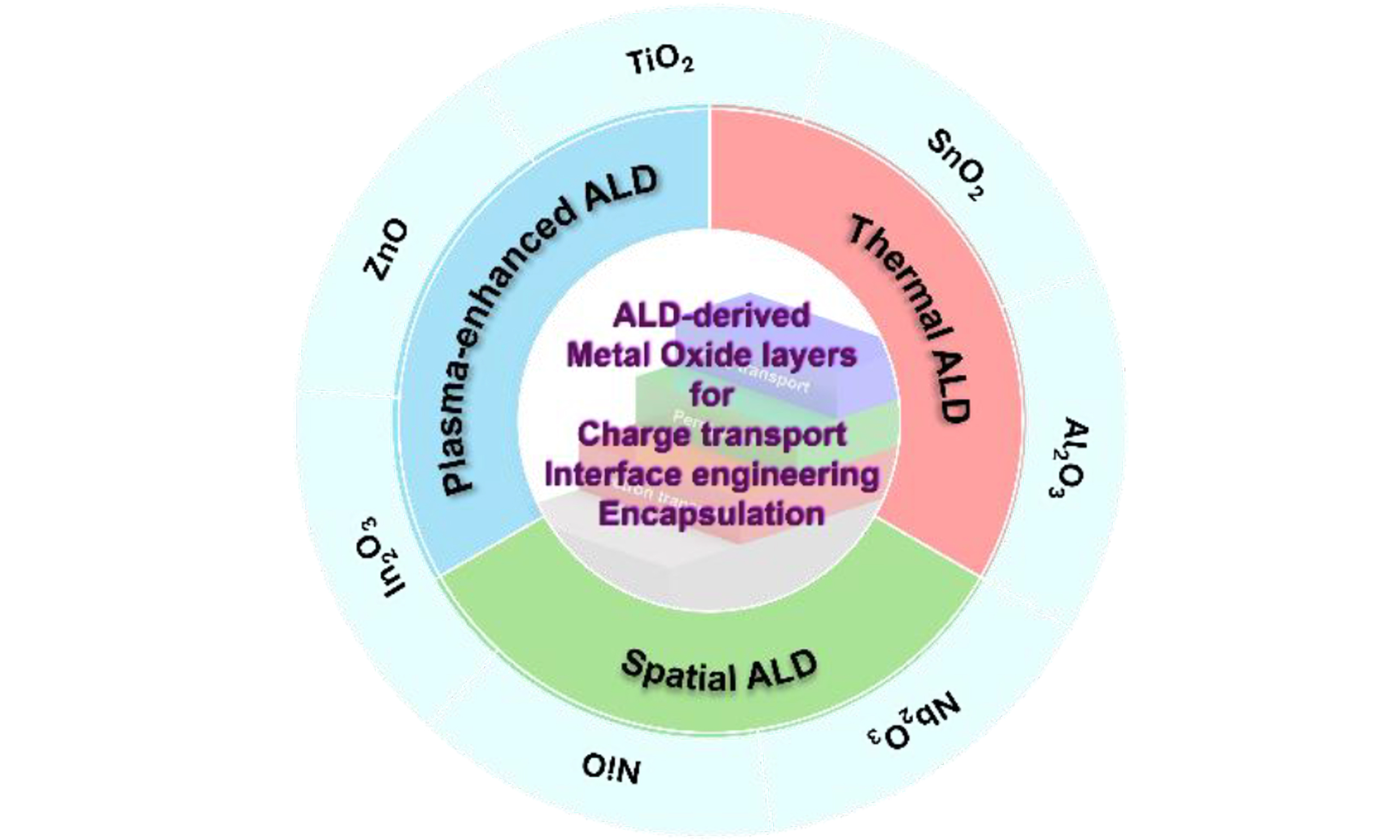
This review focuses on strategies to simultaneously enhance the efficiency and stability of PSCs through the application of MO layers fabricated via ALD. It begins by introducing the fundamental mechanisms and process characteristics of ALD, followed by a systematic analysis of the structural features of PSCs and the intrinsic instabilities of their constituent materials. Subsequently, representative cases of ALD MO thin film and their corresponding effects are summarized, with particular emphasis on approaches to overcome environmental stress factors and intrinsic degradation pathways. The review then provides an in-depth discussion of the synergistic effects enabled by the incorporation of ALD-derived MO layers, along with process optimization strategies, prospects for large-area fabrication, and pathways toward industrial-scale implementation. Finally, the remaining challenges that should be addressed for commercialization are highlighted, including precise control of film properties, process compatibility, cost-effectiveness, and scalable manufacturing infrastructure. Overcoming the intrinsic instabilities of PSCs and establishing efficient and sustainable PV systems will require the strategic design and implementation of ALD-based MO layers. By comprehensively addressing these technical challenges, this review aims to provide a roadmap for the stable and sustainable advancement of PSCs by ALD MO [Figure 1].
Figure 1. Schematic illustration of ALD MO-based PSC system for improving PCE and stability.
WORKING PRINCIPLES AND KEY FEATURES OF ALD IN PSC
Minimizing efficiency losses and degradation in PSCs requires precise defect management and effective suppression of degradation pathways. ALD has emerged as a promising technique capable of meeting these demands and has already been utilized in a variety of photovoltaic technologies, including perovskite, Si, III-V, CdTe, CIGS, organic, and dye-sensitized solar cells (DSSCs)[62-64]. Owing to its suitability for depositing a wide range of thin films including MOs and nitrides, ALD offers significant advantages for device
ALD fundamentals and process framework
ALD is a sophisticated thin-film deposition technique that relies on self-limiting reactions between precursors and substrate surfaces. This system enables the growth of ultrathin and highly uniform films with atomic-scale thickness control, while also ensuring conformality on substrates with complex surface geometries[66-68]. The basic protocol of ALD process consists of four sequential steps that together form one cycle, illustrated in Figure 2. First, precursors such as an organometallic compound are introduced into the evacuated reaction chamber and pulsed onto the substrate where they adsorb. The primary adsorption mechanism in ALD is chemisorption, where chemical bonds form between the precursor and reactive surface sites, in contrast to the weaker physisorption governed by van der Waals interactions or hydrogen bonding[69]. Once the surface is saturated with the precursor, the reaction ceases, demonstrating the self-limiting nature of ALD[70,71]. The chamber is then purged with an inert gas to remove unreacted precursors and volatile by-products. In the next, oxidizing agent as a second precursor is pulsed into the chamber to react with the chemisorbed species. This forms the desired thin film material while simultaneously regenerating reactive surface sites for the next cycle[72]. By repeating these steps, the film thickness can be precisely controlled.
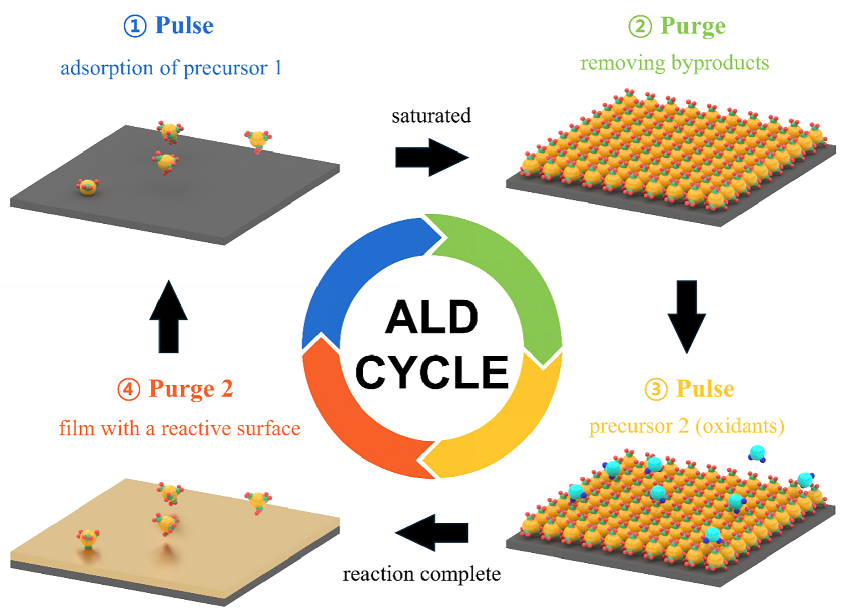
Figure 2. Schematic illustration of ALD process.
ALD offers a clear advantage in conformality compared with solution-based processes and other vapor deposition widely used for PSC fabrication. Solution processes are often hindered by surface tension and viscosity effects, which limit infiltration into nanoscale features and lead to non-uniform film formation[73-75]. Whereas ALD employs gaseous precursors, enabling highly conformal coverage. Nattoo et al. carried out a comparative study of molybdenum disulfide (MoS2) thin films prepared by low-temperature ALD and radio frequency (RF) sputtering focusing on their optical, structural, surface, and electronic properties[76]. Raman spectroscopy showed that sputtered MoS2 has weaker and broader Raman peaks, which indicates a higher concentration of defects, while the ALD films exhibited sharper features consistent with enhanced crystallinity. Transmission electron microscopy (TEM) further supported this distinction: the ALD films maintained a relatively uniform structure consisting of three to four layers, whereas the sputtered films displayed noticeable nonuniformity with amorphous MoOx appearing at the substrate interface. Additional findings such as reduced surface roughness, higher current density, and improved mobility in the ALD samples confirmed that the ALD process is more suitable for achieving high-quality MoS2 thin films. This capability is particularly advantageous for depositing MOs, which are essential components in PSCs and other electronic devices due to their unique properties, tunable structures, and versatile functionality[77]. Importantly, the bandgap, composition, and nanostructure of ALD MOs can be precisely tailored to meet diverse device requirements[78-80]. The chemisorption of MO precursors in ALD typically proceeds via ligand-exchange reactions with surface groups. For instance, in the deposition of tin oxide (SnO2), tetrakis(dimethylamino)tin(IV) (TDMASn) as a Sn precursor reacts with surface hydroxyl groups (-OH), resulting in the adsorption of Sn and the release of volatile dimethylamine[81]. Once surface saturation is achieved, the chamber is purged and H2O is introduced as an oxidizing agent. The H2O reacts with the surface-bound ligands, forming Sn-O bonds while simultaneously regenerating -OH, thereby preparing the substrate for the next cycle[82].
A key limitation of thermal ALD is its requirement for elevated temperatures to activate the self-limiting reactions, which restricts its application on thermally sensitive substrates[83]. Plasma-enhanced ALD (PEALD) has been developed to address this issue by generating highly reactive radicals that drive surface reactions at low temperature[84,85]. This reduces thermal damage, making the process suitable for organic layers and completed devices, including flexible PVs[86,87]. However, the lower processing temperatures of PEALD can compromise precursor reactivity, often leading to the incorporation of carbon and nitrogen impurities and the formation of amorphous or polycrystalline films with reduced electrical conductivity[88]. Optimizing PEALD parameters including process temperature, plasma conditions, and pulse times can help mitigate these limitations, as these variables strongly influence film crystallinity, impurity content, density, and uniformity. For example, Xu et al. systematically compared the film growth behavior, microstructural characteristics, and electrical properties of SnO2 thin films deposited on Si wafers via thermal ALD, PEALD, and layer-by-layer Ar plasma treatment (PEALD-ALT)[89]. All films were deposited at 250 °C using TDMASn as the Sn precursor, while O3, O2 plasma, and an additional Ar plasma step were employed as oxidants depending on the deposition route. All processes exhibited self-limiting growth behavior; however, due to the enhanced reaction activity of O2 plasma, the growth per cycle (GPC) was highest for PEALD. In contrast, PEALD-ALT showed a slightly reduced GPC, attributed to partial surface etching during the subsequent Ar plasma treatment. The thermal ALD film exhibited low crystallinity, whereas the PEALD film favored SnO2 growth along the (220) orientation. In the case of PEALD-ALT SnO2, the dominant (221) orientation was observed, which was ascribed to enhanced surface atom mobility and subsequent surface reorientation induced by Ar plasma exposure. The PEALD-ALT SnO2 film, with increased oxygen vacancy concentration and improved crystallinity, achieved the lowest resistivity of 1.80 × 10⁻³ Ω·cm, significantly lower than that of the thermal ALD film (15.3 × 10⁻³ Ω·cm), indicating improved electrical conductivity. Nevertheless, physical ion bombardment, grain growth, densification, and local temperature rise during plasma treatment introduced substantial residual stress, leading to increased surface cracking and roughness. Overall, this approach enables the growth of highly conductive and crystalline SnO2 films without high-temperature post-annealing, offering a promising route for fabricating transparent conductive oxides and charge-transport layers suitable for flexible or thermally sensitive optoelectronic devices.
ALD requires a long processing time because precursor pulsing and chamber purging need to be repeated for every cycle[90,91]. As the desired film thickness increases, the required number of cycles rises proportionally, making throughput a critical challenge for large-scale production. Spatial ALD (SALD) has been introduced as a promising solution to the bottleneck. Apart from conventional ALD where precursors and purging gases are introduced sequentially within a single chamber, spatial ALD separates these steps into distinct areas[92,93]. As the substrate continuously moves through separated zones, adsorption and purging occur in parallel, eliminating downtime between pulses and enabling high-speed deposition. This continuous process accelerates growth rates and is also compatible with roll-to-roll process, thereby facilitating scalable deposition on large-area and flexible substrates[94]. Notably, while SALD ensures reasonable thickness control and uniformity through self-limiting reactions, it inherently necessitates complex reactor architectures, stringent gas flow regulation, and meticulous optimization of operational parameters such as substrate movement speed and gas flux, thereby elevating the overall process complexity[95,96]. For instance, Jiang et al. adopted SALD to circumvent the chamber-size limitations and slow cycling speed of thermal ALD for large-area SnO2 film growth[97]. The process was carried out at 100 °C to ensure compatibility with perovskite layers, oxidants with different reactivities were compared using TDMASn as the tin precursor. The oxidation state and vacancy concentration were effectively regulated by varying the oxygen sources. The GPC of SnO2 with H2O2 was 2.05 Å cycle-1, and saturation growth was observed when the TDMASn and H2O2 flow rates were set to 250 and 50 sccm. Moreover, the substrate transport velocity and the nozzle-substrate spacing (micro-gap) were optimized as key process parameters. At a substrate velocity of 75 mm/s, the thickness nonuniformity across a 20 × 20 cm2 substrate was minimized to 2.24 %. When the micro-gap was increased beyond 1.0 mm, the precursors injected from adjacent channels intermingled, leading to enhanced CVD-type growth and a consequent decrease in film uniformity. The optimization of precursor type, reactivity, substrate transport, and reaction-zone width in SALD is essential to achieving uniform film thickness, smooth surface morphology, and desirable electrical properties such as high carrier mobility and low resistivity.
Despite several challenges, ALD remains one of the most precise and versatile deposition techniques available. With its ability to finely tune film properties and ensure excellent conformality, ALD encompassing both conventional and spatial approaches offers significant potential for enhancing the efficiency and stability of PSCs while simultaneously providing a scalable pathway for industrial applications and large-area device fabrication.
Configuration of PSCs
Typical PSCs are generally categorized into the two architectures, namely regular (n-i-p) and inverted (p-i-n), according to the deposition sequence of the charge transport layers (CTLs) on the transparent conducting oxide (TCO). Both structures are composed of five basic layers, which include the electrodes, CTLs, and perovskite absorber [Figure 3A and B]. Upon illumination, the perovskite layer generates charge carriers, which are separated and transported through the respective CTLs to be collected at the electrodes. Halide perovskites are crystalline materials with the formula ABX3, where the A site is occupied by a monovalent organic or inorganic cation, the B site by a divalent cation such as Pb2+ or Sn2+, and the X site by a halide anion[98,99] [Figure 3C]. Calculated from the ionic radii of the constituent ions, the Goldschmidt tolerance factor (t) serves as an indicator of perovskite structural stability. A value near ~1 suggests the formation of an ideal cubic phase[100]. The framework of corner-sharing [BX6] octahedra provides pathways for charge carriers generated by light absorption[101]. The valence band (VB) and conduction band (CB) are derived from orbital interactions between B- and X-site ions, while the A-site cation indirectly influences band structure by modifying B-X bond lengths and angles[102]. As a result, halide perovskites exhibit a direct bandgap that facilitates efficient charge carrier generation without requiring momentum change, and their bandgap can be readily tuned by halide substitution[103]. For example, replacing I- with Cl- increases the bandgap from ~1.5 to ~2.4 eV due to altered orbital overlap between halide anions and B-site cations[104]. Similarly, replacing Pb2+ with Sn2+ enhances s-p antibonding within the octahedra, leading to a bandgap reduction[105]. This endows halide perovskites with strong optical absorption, ambipolar charge transport, and convenient solution processability, making them attractive absorber materials for high-efficiency solar cells.
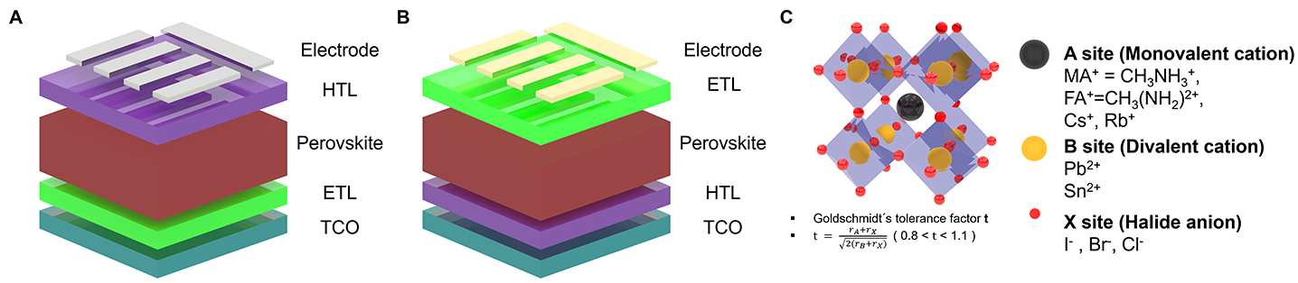
Figure 3. (A) Device structures of regular and (B) inverted PSCs. (C) Schematic illustration of halide perovskite structure.
Despite their outstanding optoelectronic properties, perovskites suffer from intrinsic and environmental instabilities that limit device operation. The photoactive cubic α-phase of FAPbI3 which is suitable for light harvesting is thermodynamically unstable at room temperature and tends to convert into the photoinactive hexagonal δ-phase[106]. In addition, the soft ionic lattice results in low defect formation energies, enabling facile migration of organic cations and halide anions[107]. This generates a high density of vacancies, interstitials, and substitutional defects, which act as nonradiative recombination centers and exacerbate ion migration. Such instabilities are further accelerated under operational conditions by exposure to light, moisture, and heat[108]. Light and heat promote volatilization of organic cations and activate ion migration, while water molecules irreversibly hydrolyze perovskites into precursors such as organic salts and PbI2[109]. Grain boundaries and defects in perovskite films provide diffusion pathways for moisture ingress, while oxygen and illumination lower the activation energy for decomposition and perpetuate degradation cycles[110,111].
Strategies comprising compositional engineering in which A-site cations or halide anions are mixed to stabilize the lattice together with the introduction of additives during film growth to suppress defect formation, can mitigate these issues but do not fundamentally resolve the thermodynamic instability of the material[112,113]. As a result, interface engineering has emerged as an additional strategy to improve both efficiency and stability, through the introduction of interlayers or surface modifications at the perovskite/CTL interface[114,115]. MOs are considered highly attractive materials because of their chemical robustness and long-term durability. They passivate interfacial defects, impede the permeation of moisture and oxygen, and suppress degradation induced by ion migration between metal electrodes and neighboring layers[116-118]. Owing to beneficial functionalities, MOs function both as buffer layers and as encapsulation materials that shield the device from external environments[93,119]. MOs exhibit efficient charge transport because oxygen vacancies act as electron-donating defects in n-type MOs, while metal-ion deficiencies generate holes in their p-type counterparts[120]. Owing to their inherently high carrier mobility and tunable semiconducting behavior, MOs can also be readily engineered into diverse nanostructures. MOs are particularly attractive for low-cost, large-area fabrication, and their thin-film properties such as crystallinity, particle size, and defect concentration can be finely adjusted through process parameters including annealing temperature and atmosphere. These characteristics can be further optimized by controlling deposition temperature and pressure in a range of vapor-phase deposition methods.
In PSCs, CTLs are typically constructed from either organic materials or MOs. Common electron transport layer (ETL) materials include fullerene (C60) and derivatives such as phenyl-C61-butyric acid methyl ester (PCBM), as well as n-type MOs such as TiO2, SnO2, and zinc oxide (ZnO)[121,122]. For hole transport layers (HTLs), conductive polymers such as poly(3,4-ethylenedioxythiophene):poly(styrenesulfonate) (PEDOT:PSS), small molecules like 2,2′,7,7′-tetrakis(N,N-di-p-methoxyphenyl-amine)9,9′-spirobifluorene (spiro-OMeTAD), and p-type MOs such as nickel oxide (NiO) are widely employed[123-125]. Although TiO2 exhibits excellent optical properties and chemical stability, its low conductivity limits its applicability as an efficient charge-transport layer in PSCs[126]. SnO2, by contrast, provides high electrical conductivity and strong adhesion to flexible polymer substrates, which helps prevent delamination and cracking and thereby enhances mechanical reliability[127]. Both MOs exhibit outstanding chemical stability and high electron mobility, making them suitable as electron-transport and buffer layers in solar cells and ferroelectric devices. ZnO allows wide tunability of n-type conductivity and resistivity through doping and defect engineering, and it can be synthesized in various nanostructures[128]. The strong piezoelectric properties further enable applications in energy harvesting, sensing, and other electronic devices. The appropriate materials designated for CTLs need to exhibit appropriate energy-level alignment, high conductivity, and sufficient carrier mobility, with the specific selection depending on whether the device is fabricated in the regular or inverted configuration. In regular devices, the ETL is deposited directly on the TCO and can therefore tolerate high-temperature processing. Typically MOs require temperatures above 150 °C, and NiO can also be employed under similar high-temperature conditions in HTL of inverted structure[129]. MOs are advantageous due to their chemical and thermal stability, energy-level compatibility with perovskites, and ability to be fabricated via simple spin-coating process[130]. However, the requirement for high-temperature annealing and the limited solvent choices restrict their application as regular HTLs, inverted ETLs, or in flexible device. Organic CTLs can be deposited at low temperatures, making them more compatible with perovskite layers and polymeric substrates[131]. For instance, spiro-OMeTAD commonly used as an HTL in regular structures is formed without any annealing and offers favorable energy-level alignment with perovskite absorbers[132]. In inverted structures, HTLs must be stable against both high-temperature annealing (≥ 100 °C) and polar solvents such as dimethylformamide (DMF), making PEDOT:PSS, PTAA, and carbazole-based self-assembled monolayers (SAMs) such as [2-(9H-carbazol-9-yl)ethyl]phosphonic acid (2PACz) suitable options[133].
Nevertheless, organic CTLs face limitations including high cost due to complex synthesis and purification, the need for additional dopants to improve charge transport, and poor stability under operational conditions. Spiro-OMeTAD requires Bis(trifluoromethane)sulfonimide lithium and cobalt salts (Li-TFSI, Co-TFSI) to compensate for low hole mobility, yet these metal ions can migrate into perovskite vacancies and impair stability[134]. Fullerene-based ETLs also suffer from limited tunability of energy levels and poor photostability[135].
With the aim of mitigating the issues, inorganic MOs with superior intrinsic properties can be deposited directly onto perovskite layers or flexible substrates by ALD. ALD MO layers exhibit low pinhole density, high compactness, and effective barrier properties against moisture and oxygen, thereby improving both efficiency and stability[136]. Moreover, ALD layers can function not only as standalone CTLs but also as bilayer structures in combination with solution-processed CTLs, as interfacial or buffer layers between the perovskite and CTLs, or between CTLs and electrodes[77,137]. Al2O3 with insulating nature from wide bandgap hardly serve as an electron transport material but can act as a hole-blocking and defect-passivating interlayer. Owing to chemical and thermal stability, it can also be applied as a thin buffer layer or in encapsulation to enhance device lifetime. Despite their chemical stability, metal top electrodes are prone to degradation through the formation of metal halides driven by ion migration under illumination[138]. The insertion of ALD MO buffer layers between HTLs and metal electrodes suppresses such reactions and improves thermal stability[139]. Encapsulation processes incorporating MOs also play a crucial role in preventing direct exposure of perovskites to moisture and oxygen. While organic encapsulants such as ethylene vinyl acetate (EVA), poly(ethylene terephthalate) (PET), and epoxy resins are mechanically flexible and compatible with low-temperature processing, they provide insufficient barrier performance compared to inorganic oxides[140,141]. ALD MOs fabricated at low temperature thus presents an effective solution for encapsulation, offering superior moisture and oxygen impermeability without compromising device integrity[142]. Indeed, the insufficient stability of perovskite absorbers necessitate the incorporation of additional interfacial and barrier layers within PSC architectures. ALD MOs with defect passivation capability, robust stability, and barrier properties represent a particularly effective strategy to simultaneously enhance the efficiency, durability, and scalability of perovskite solar cells.
APPLICATION OF ALD MO IN PSC
The efficiency and stability of PSCs are strongly dependent on the optoelectronic, physical, and chemical properties of the constituent layers. Over the past several years, approaches informed by fundamental insights into perovskite degradation mechanisms and charge carrier dynamics have led to significant improvements in device efficiency[143]. Nevertheless, the intrinsic instability of perovskite materials arising from their weak ionic bonding remains a major challenge, particularly with respect to vulnerability against external factors such as moisture and oxygen[144]. In addition to improving the crystallinity of the perovskite absorber itself, interfacial modification through the incorporation of interlayers and the introduction of encapsulation strategies have been proposed as effective means to enhance device stability[42]. Accordingly, the materials used in layers of PSC should provide excellent chemical and physical stability, control interfacial defects without hindering light absorption or charge transport, and offer long-term durability. MOs with high environmental resistance represent highly promising candidates for device fabrication. The valence band maximum (VBM) of MO is typically derived from O 2p orbitals, while the conduction band minimum (CBM) arises from the outer orbitals of metal cations[145]. The resulting large energy separation generally renders them wide-bandgap semiconductors. Since the bonding characteristics, crystal structures, and oxidation states vary depending on the metal cation, appropriate MOs can be selected for each functional layer of PSCs. For instance, SnO2, TiO2, and NiO are semiconductors whose energy levels align well with perovskite absorbers, allowing efficient electron or hole extraction and transport[146]. In contrast, Al2O3 with a bandgap exceeding 7.0 eV is an insulator unsuitable for CTLs but highly chemically stable, thus serving effectively as a barrier against unwanted penetration of external species[147]. Solution-based deposition of MOs, however, often requires high-temperature annealing for crystallization, introducing defects and impurities[148]. The ALD MOs provide uniform and conformal films with atomic-scale thickness control, offering a promising approach to overcome the limitations. This section will examine the roles of ALD MO layers in PSCs and the specific characteristics of the associated processes.
ALD MO layer deposition for TCO electrodes
The front contact of PSC should maximize light transmission to the perovskite absorber while simultaneously ensuring proper energy-level alignment with CTLs. TCOs are employed as their wide bandgap provides optical transparency without hindering light absorption, while doping with elements such as Sn or fluorine (F) confers high electrical conductivity[149,150]. TCOs also offer excellent chemical stability and durability, making them compatible with high-temperature processing. Among single-junction PSCs, indium tin oxide (ITO) and fluorine-doped tin oxide (FTO) are the most commonly used transparent electrodes[151]. The transparent films can be prepared through various techniques including spray pyrolysis, TE, and CVD, with magnetron sputtering-produced ITO-coated glass serving as a representative large-area substrate[152]. Although these processes ensure reasonable reproducibility, uniformity, and deposition speed, the utilization of ALD confers exceptional control of surface chemical properties. The surface of conventional ITO typically contains hydroxyl groups bound through both physical adsorption and chemisorption[153]. However, when the OH group forming weak hydrogen bonds is lost during the processes, the functional group of the SAM-based HTLs fails to anchor to the surface of substrate, resulting in reduced coverage[154]. To address this, Tang et al. introduced ITO films modified by ALD using TDMASn and trimethylindium precursors to prevent the desorption of OH groups caused by strong polar solvents[155]. The resulting ALD ITO fabricated by alternating cycles of In2O3 and SnO2 deposition preserved a high density of covalently bound hydroxyl groups even after DMF treatment. MeO-2PACz and (3,6-dimethoxy-9H-carbazol-9-yl)trimethoxyphenylsilane (DC-TMPS) as SAM HTL were subsequently immobilized on the ALD ITO surface. While MeO-2PACz features a bidentate phosphonic acid anchoring group, DC-TMPS incorporates a tridentate trimethoxysilane group, which forms stronger bonds with surface hydroxyls. As a result, both molecules improved the power conversion efficiency (PCE) of PSCs fabricated on ALD ITO substrates, but DC-TMPS in particular yielded superior enhancements in light and thermal stability. In contrast to ITO, which relies on the expensive and scarce element indium, aluminum-doped zinc oxide (AZO) is composed of abundant, nontoxic elements (Zn and Al), making it a low-cost alternative[156-158]. de Melo Monteiro Modesto et al. reported ALD-grown AZO films using diethylzinc (DEZ) and trimethylaluminum (TMA) as Zn and Al precursors[159]. The resulting AZO exhibited over 80% transmittance in the visible region, a bandgap greater than 3.3 eV, and a low resistivity of 1.26 × 10⁻² Ω·cm, indicating its potential as an effective TCO layer for enhancing light absorption and charge transport in PSCs. Despite these promising results, however, the electrical conductivity and optical transmittance of AZO remain inferior to those of ITO and FTO, underscoring the need for further optimization.
ALD MO layer deposition for CTLs
MOs for ETL
The ETL in PSCs is expected to be capable of electron extraction and hole blocking, in addition to offering high electron mobility, optical transmittance, facile and uniform film formation, and chemical stability. On account of the demanding requirements, the materials employed as ETLs have been selectively chosen depending on the device architecture. In regular type PSCs, the ETL is fabricated prior to the perovskite layer, and therefore high-temperature annealing can be employed. Although this limits the use of flexible substrates, MO-based ETLs such as SnO2 and TiO2 fabricated through high-temperature processing fulfill most of the required conditions. More recently, advances in sol-gel precursor design and quantum dot (QD) solution processing have facilitated the low-temperature (< 150 °C) formation of MO ETL, yet film non-uniformity and surface/bulk defects continue to persist[160,161].
As a process to improve the quality of ETLs, ALD can provide highly pure and conformal thin films without defects and offers precise control at the atomic scale as well as the ability to modify chemical properties through doping or precursor adjustment, being applied either alone or in combination with solution processes. Hsu et al. fabricated tantalum (Ta)-doped TiO2 films to improve the conduction-band mismatch and high resistivity of TiO2 ETL[162]. By simultaneously introducing titanium isopropoxide (TTIP) and tantalum ethoxide (Ta(OEt)5) precursors and controlling the Ta concentration by adjusting the bubbler temperature in the range of 70-90 °C, Ta-doped TiO2 films were deposited through PEALD. This process induced the formation of oxygen vacancies, reduced the bandgap from 3.17 to 3.0 eV, and shifted the conduction band downward, thereby decreasing the resistivity to the level of 10-1 Ω·cm. XPS results confirmed the reduction of Ti4+ to Ti3+ and Ti2+, accompanied by oxygen vacancies acting as donor levels, which increased the free electron concentration [Figure 4A]. Devices based on the improved ETL exhibited a PCE increase from 13.4% to 18.1%, while the hysteresis index (HI) decreased from 1.06% to 0.21%. When excessive Ta doping was introduced due to overly high bubbler temperatures, defect formation increased and efficiency decreased. Chai et al. introduced ALD TiO2 to overcome difficulties in completely covering the rough FTO substrate with solution-processed TiO2 ETL[163]. The ALD TiO2 fully covered the protrusions of the FTO surface, suppressing leakage current. The solution-processed TiO2 deposited on top elevated the CBM, forming better energy-level alignment with the perovskite layer [Figure 4B]. Steady-state PL (ssPL) spectra showed that the PL peaks of CsPbI3 deposited on TiO2 bilayers were blue-shifted, confirming improved crystallinity [Figure 4C]. As a result, the device incorporating ALD TiO2 exhibited enhanced electron transport, increasing the PCE from 18.80% to 19.60% and maintaining stable output under operational conditions. Nb-doped TiO2 ETLs were fabricated by adjusting the ratio of Ti and Nb sources, where the incorporation of Nb atoms into the TiO2 lattice caused lattice expansion[164]. Through a supercycle ALD process with TTIP, tris(diethylamido)(tert-butylimido)niobium(V) (TBTDEN), and H2O precursors, the Nb incorporation was controlled. The sequence of Ti-H2O-Nb-H2O proved to achieve the most stable Nb doping. The deposited films were controlled to a thickness of 15 nm, and upon annealing at 500 °C, the anatase crystalline phase was formed, improving the electronic structure and optical properties. With increasing Nb content in the ALD TiO2, Jsc, Voc, and FF improved, and under optimized conditions, the PCE reached 18.3%, surpassing that of pristine TiO2 (16.2%) and Nb2O5 (16.45%). In stability assessments, the devices retained ~17.6% efficiency after 61 days of shelf aging and maintained 80% of their initial performance after 138 h under continuous illumination under ISOS-L1 conditions. In conclusion, the doping concentration in TiO2 ETLs must be precisely controlled, and ALD demonstrates its effectiveness in achieving such fine-tuned optimization.
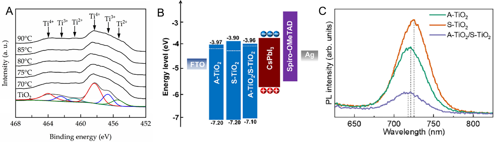
Figure 4. (A) O 1s core-level spectra from XPS analysis of Ta-doped PEALD-grown TiO2 thin films at varying bubbler temperatures[162]. Copyright 2021, MDPI. (B) Energy band diagram of ALD (A-)/solution(S-)/bilayer TiO2 ETL-based devices[163]. Copyright 2023, Elsevier. (C) ssPL spectra of A-/S-/bilayer TiO2 film[163]. Copyright 2023, Elsevier.
SnO2 generally exhibits higher electron mobility than TiO2 and provides better conduction band alignment with perovskite absorbers, while also being deposited at lower temperatures[165,166]. Due to suppressed charge recombination losses, highly efficient regular type PSCs frequently employ SnO2 as the ETL[167,168]. SnO2 is usually deposited by solution-based methods involving sol-gel, colloidal nanoparticle dispersion, and chemical bath deposition (CBD), which are cost-effective and compatible with large-area production. However, these approaches often face challenges with film uniformity and thickness control, and they readily introduce surface defects such as impurities and oxygen vacancies that act as trap sites, thereby reducing electron extraction efficiency[169,170]. Incorporation of ALD helps overcome such issues, promoting the high-quality SnO2 even at low temperatures through careful control of process parameters. Above a certain temperature threshold, ALD SnO2 growth deviates from self-limiting behavior and transitions toward CVD-like deposition[171]. Although oxygen vacancies can increase carrier density, they simultaneously reduce mobility due to enhanced scattering[172]. Therefore, a balance of thermal energy and optimized processing conditions is required to activate surface reactions for uniform film growth while minimizing defect formation. Martinez-Puente et al. optimized process conditions for remote and direct plasma ALD (RPALD and DPALD) of SnO2 using TDMASn and oxidants[173]. When hydrogen unintentionally substituted for oxygen vacancies, it acted as a shallow donor and induced surface plasmon resonance (SPR). The hot electrons generated by SPR were injected into the SnO2/perovskite interface, promoting photocatalysis. However, doping was minimized under RPALD conditions at 80 °C with O2 as the oxidant. While the growth of the ALD SnO2 can be precisely controlled, SnO2 often performs better when fabricated as a bilayer in combination with solution-based methods rather than solely by ALD when applied to the TCO in regular type PSCs. Gong et al. analyzed the challenges associated with coating ITO using ALD SnO2[174]. Interestingly, the roughness of the ALD SnO2 film was found to be higher than that of both bare ITO and solution-processed SnO2, which resulted in a reduced charge transport efficiency in the device. The observed roughness increase was attributed to the inherent nature of ALD, as the repeated atomic-scale deposition process tends to amplify the pre-existing surface irregularities of the ITO. In contrast, spin-coating a solution allows the film to spread and self-level across the substrate surface. Conversely, the bilayer SnO2 film - fabricated by subsequently depositing a solution-processed layer on top of the ALD layer - exhibited the lowest roughness. This improvement was attributed to the initial ALD layer enhancing the chemical affinity between the substrate and the solution, thereby enabling a more uniform coating. The charge extraction efficiency of the various SnO2 coatings was further investigated using time-resolved photoluminescence (TRPL) spectroscopy on ITO/SnO2/perovskite films. The TRPL results revealed that the ALD-coated film exhibited a shorter decay time compared with the spin-coated film, indicating more efficient charge transfer at the interface. Zhang et al. also combined with sol-gel derived SnO2 in a bilayer suppressed colloidal aggregation, reduced surface roughness, and increased the contact angle, improving PbI2 crystallization[175] [Figure 5A]. Grazing-incidence wide-angle X-ray scattering (GIWAXS) confirmed superior orientation and intensity of the bilayer-derived PbI2 films, as indicated by (100) plane azimuthal cuts [Figure 5B and C]. TRPL measurements revealed a notable reduction in decay components. The fast decay lifetime (τ1) corresponding to electron transfer from the perovskite to the interface decreased from 18.53 ns for the sol-gel SnO2 film to 10.10 ns for the bilayer film. Similarly, the slower recombination component (τ2), associated with defect-mediated recombination, declined from 71.32 to 38.12 ns. Consequently, the average carrier lifetime shortened from 60.20 to 30.61 ns. The accelerated PL decay indicates more efficient electron extraction into the ETL and reduced defect-assisted recombination. Furthermore, XPS analysis of the O 1s and Sn 3d core levels confirmed improved interface stability. The XPS spectra showed an increased Sn4+/Sn2+ ratio and a lower density of surface oxygen vacancies, evidencing enhanced film stoichiometry and reduced interfacial defects. Consequently, the champion device achieved a PCE of 23.86%, representing enhancement over the 22.09% control. Ge et al. introduced V-shaped nanoplate FTO (NP-FTO) substrates to mitigate energy losses from oblique light incidence and nonradiative recombination associated with conventional ITO and FTO[176]. Integrating sphere and angle-resolved reflection (ARR) measurements showed suppressed reflectance across a wide spectral range (500-800 nm) and angles (-50° to 50°) due to the formation of a graded refractive index. Enhanced perovskite crystallization and improved carrier lifetimes were also observed. To cover the rough NP-FTO surface, SnO2 was deposited by ALD, followed by spin-coated SnO2 quantum dot films to form a bilayer ETL. Using TDMASn at 95 °C and H2O at 45 °C, a 4 nm SnO2 film was deposited over 24 cycles at 90 °C and then annealed at 150 °C for 30 min, producing a uniform, compact layer that prevented direct exposure of the substrate to the perovskite solution. This conformal ALD layer, integrated with the optically favorable NP-FTO substrate, enabled devices to reach a PCE of 26.4%, with tandem cells achieving a record efficiency of 28.2%. Chen et al. analyzed the influence of ALD SnO2 on sol-gel processing, highlighting the advantages of bilayer structures[177]. Contact angle measurements showed enhanced wettability of sol-gel solutions on ALD SnO2, decreasing from 37° to 21°, which facilitated smoother film growth [Figure 5D and E]. XPS analysis revealed that ALD SnO2 exhibited a lower Sn4+/Sn2+ ratio of 1.20 compared to 1.62 in single SnO2, resulting in a lower refractive index (n). The reduced n value improved light transmittance, while enhanced perovskite crystallinity further minimized recombination losses, leading to a PCE of 20.55%. In stability tests under 1-sun white LED illumination in N2, bilayer SnO2 retained 91.47% of its initial efficiency after 1,000 h, compared with only 71.95% for the single-layer device.
Figure 5. (A) Illustration of regular structure PSC[175]. Copyright 2023, Wiley. (B) Azimuthal plots of solution[175]. Copyright 2023, Wiley. (C) Azimuthal plots of ALD/solution bilayer SnO2[175]. Copyright 2023, Wiley. (D) 3D atomic force microscopy (AFM) surface topography images of solution[177]. Copyright 2025, Wiley. (E) 3D AFM surface topography images of ALD/solution bilayer SnO2[177]. Copyright 2025, Wiley. (F) Cross-sectional TEM images of control Si/SnO2/Au film[179]. Copyright 2025, Wiley. (G) Cross-sectional TEM images of UV exposure after 15 min of Si/SnO2/Au film[179]. Copyright 2025, Wiley.
ZnO is used less frequently than TiO2 and SnO2 despite its electron mobility and low-cost nanostructure synthesis. Its limited utilization arises from abundant Zn-related donor defects and oxygen vacancies that promote electron recombination and from strong reactivity with perovskite cations[181,182]. Fournier et al. deposited compact, conformal ZnO by ALD and functionalized the surface with phosphonic acid derivatives, including 2-aminoethylphosphonic acid (2-AEPA), 4-aminobenzylphosphonic acid, and 4-fluorobenzylphosphonic acid (4-FBzPA) to address chemical instability and thermal degradation[183]. The derivatives bonded to surface -OH groups, modifying the interface [Figure 6A]. AEPA induced uniform perovskite crystallization but restricted electron extraction due to insulating characteristics, while 4-FBzPA partially covered ZnO yet effectively suppressed degradation without hindering charge transport. These results demonstrate that ALD ZnO surfaces are able to be well-functionalized for effective interface engineering. Su et al. fabricated ZnO-SnO2 bilayer ETLs by sequentially depositing ZnO and SnO2 with
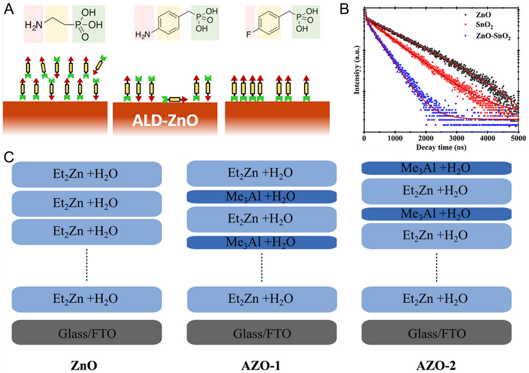
Figure 6. (A) Schematic representation of functionalized ALD ZnO surface with phosphonic acid derivatives[183]. Copyright 2021, American Chemical Society. (B) TRPL spectra of perovskite films deposited on different ETLs[184]. Copyright 2023, Wiley. (C) Schematic illustration of ALD processes with different terminate cycles[157]. Copyright 2022, Wiley.
In inverted PSCs, ETLs are deposited on top of perovskite absorbers, limiting the use of high-temperature processing. Organic ETLs such as PCBM, polyethylenimine ethoxylated (PEIE) and C60 are stable in polar solvents and commonly used to avoid perovskite damage but their high cost and poor stability motivate the introduction of inorganic MOs[122,186]. Since SnO2 can be formed at low temperatures, Rakheja et al. deposited ALD SnO2 directly onto perovskite layers in inverted PSC[187]. When deposited directly at 90 °C on FAPbI3 or FAPbBr3, ALD SnO2 induced S-shaped J-V curves. Inserting PCBM as a buffer layer between SnO2 and perovskite mitigated the low FF. XRD confirmed the formation PbI2 in FAPbI3 without major structural change, while Pb 4f5/2 peaks consistent with this decomposition in XPS. In FAPbBr3, peak broadening in Br 3d and Sn 3d spectra, along with FA decomposition signals in N 1s, indicated the formation of Sn-Br bonds and decomposition pathways. These suggest that ALD SnO2 deposition on perovskite surfaces promotes PbI2 formation in FAPbI3 and Sn-Br bonding in FAPbBr3, both of which introduce electron transport barriers. The decomposition of FA cations into formamidine and triazine species during interaction with TDMASn precursors underscores the need for optimized low-temperature processes, careful precursor selection, and additional interface engineering when employing MO ETLs in inverted architectures. The performance of PSCs employing ALD-derived ETLs is summarized in Table 1.
Device performance of PSCs based on ALD MO ETLs
| Device structure | Product | Precursors | Thickness (nm) | GPC (Å cycle-1) | Temperature (°C) | PCE (%) | Stability | Ref. |
| (Regular) FTO/ALD TiO2/Cs0.1(FA0.83MA0.17)0.9Pb(I0.83Br0.17)3/spiro-OMeTAD/Au | TiO2 | TTIP, Ta(OEt)5/O2 plasma | 60 | 0.284 | 250 | 18.09 | - | [162] |
| (Regular) FTO/ALD TiO2/solution TiO2/CsPbI3/spiro-OMeTAD/Ag | TiO2 | TDMATi | - | - | - | 19.60 | AM 1.5G, RH:30% T86.8 = 17 h | [163] |
| (Regular) FTO/ALD TiO2/mesoporous TiO2/Cs0.05(MA0.167FA0.833)0.95/Pb(I0.842Br0.158)3/PTAA/Au | TiO2 | TTIP, TBTDEN, H2O | 15 | - | 200 | 18.3 | AM 1.5G, N2 T55 = 138 h | [164] |
| (Regular) FTO/ALD TiO2/MAPbI3/spiro-OMeTAD/Ag | TiO2 | TDMATi. H2O | 15 | 0.5 | - | 18.2 | Dark, RH < 18% T90 > 336 h | [188] |
| (Regular) ITO/ALD TiO2/MAPbI3/spiro-OMeTAD/WO3/Ag | TiO2 | TTIP, H2O/O3 | 80 | 0.9 | 200 | ~10 | - | [189] |
| (Regular) FTO/ALD SnO2/(FAPbI3)0.78(MAPbBr3)0.14(CsPbI3)0.08/spiro-OMeTAD/Au | SnO2 | TDMASn, H2O/O2/O3 | 10 | 1.15~1.32 | 80 | 15.15 | - | [173] |
| (Regular) FTO/ALD SnO2/solution SnO2/FAPbI3/spiro-OMeTAD/Au | SnO2 | TDMASn, H2O | 5 | ~0.63 | 110 | 23.86 | Dark, N2, RH = 20% T85 = 1,300 h | [175] |
| (Regular) NP-FTO/ALD SnO2/solution SnO2/FAPbI3/spiro-OMeTAD/Au | SnO2 | TDMASn, H2O | 4 | ~1.66 | 90 | 25.9 | AM 1.5G, 55 °C, N2 T95 = 1,200 h | [176] |
| (Regular) ITO/ALD SnO2/solution SnO2/MA0.10Cs0.05FA0.85Pb(I0.78Br0.21)3/spiro-OMeTAD/Au | SnO2 | TDMASn, H2O | 3.8 | ~1.52 | 120 | 20.22 | AM 1.5G, N2 T91.47 = 1,000 h | [177] |
| (Regular) FTO/ALD SnO2/Cs0.05(MA0.166FA0.833)0.95Pb(Br0.166I0.833)3/PTAA/Au | SnO2 | TDMASn, TBTDENM, H2O | 15 | - | 100 | 13.08 | - | [178] |
| (Regular) FTO/ALD SnO2/(MAPbI3)0.95(FAPbIBr2)0.05/spiro-OMeTAD/Au | SnO2 | TDMASn, H2O | 10 | 0.63 | 125 | 22.86 | AM 1.5G, RH = 5% T87.4 = 1,000 h | [179] |
| (Regular) ITO/ALD SnO2/(FAPbI3)0.95(MAPbBr3)0.05/PTAA/Au | SnO2 | TDMASn, H2O/Ar plasma | 10 | - | < 200 | 21.8 | AM 1.5G, 85 °C, RH = 85 % T96 = 1,000h | [180] |
| (Regular) FTO/ALD SnO2/PCBM/MAPbI3/spiro-OMeTAD/Au | SnO2 | TDMASn, H2O | - | - | 120 | 19.3 | AM 1.5G, RH = 30% T80 > 100 h | [190] |
| (Regular) ITO/ALD SnO2/FAMAPb(IBr)3/spiro-OMeTAD/Ag | SnO2 | TDMASn, O3 | 15 | 0.8~0.9 @ 100~150 °C 1.7 @ 250 °C | 200 | 15.0 | - | [191] |
| (Regular) ITO/solution SnO2/ALD SnO2/FAPbI3/spiro-OMeTAD/Au | SnO2 | TDMASn, H2O | - | - | 180 | 22.12 | Dark, RH < 10% T100 = 240 h | [174] |
| (Inverted) ITO/Me-4PACz/FAPbI3/ALD SnO2/Ag | SnO2 | TDMASn, H2O | 30~35 | 1.24 | 90 | - | - | [187] |
| (Inverted) FTO/NiO/2PACz/Cs0.1MA0.02FA0.88Pb(I0.98Br0.02)3/ethenyltriethyloxysilane/solution SnO2/ALD SnO2/Au | SnO2 | TDMASn, H2O | 40 | 1 | 100 | 23.0 | Dark, 85 °C, RH = 10% T82 = 1,000 h | [192] |
| (Regular) FTO/ALD ZnO/FbzPA/Cs0.05(FA0.83 MA0.17)0.95Pb(I0.83 Br0.17)3/spiro-OMeTAD/Au | ZnO | DEZ, H2O | 10~15 | - | 150 | 4.1 | - | [183] |
| (Regular) FTO/ALD ZnO/ALD SnO2/Cs0.05FA0.8MA0.15Pb(I0.75Br0.25)3/spiro-OMeTAD/Au | ZnO, SnO2 | DEZ, TDMASn, H2O | ZnO:28 SnO2:17 | - | 120 | 18.1 | - | [184] |
| (Regular) FTO/AZO/MAPbI3/spiro-OMeTAD/Au | AZO | DEZ, TMA, H2O | 20 | - | 200 | 18.09 | - | [157] |
| (Regular) ITO/In2O3/ | In2O3 | Trimethylindium, O3 | 30 | 0.88 | 250 | 10.97 | - | [193] |
MOs for HTL
For efficient HTL design in PSCs, materials with highest occupied molecular orbital (HOMO) levels deeper than the perovskite VBM are particularly promising as they suppress electron leakage, facilitate hole extraction, and improve stability[194]. Prominent candidates demonstrating these features include NiO, CuOx, CoOx, among others[195,196]. Notably, NiO has emerged as the most widely utilized inorganic HTL due to its favorable energy level alignment, superior stability, and compatibility with a broad range of deposition techniques represented by solution processing, vacuum evaporation, sputtering, and ALD[197]. Inverted PSCs employing organic HTLs particularly carbazole-based SAMs have often exhibited higher efficiencies, which stems from the ability of organic molecules to precisely tune their HOMO levels relative to the perovskite VBM through molecular design, as well as the relative ease of enhancing hole mobility and conductivity via doping[198]. Nonetheless, inorganic MOs remain attractive for commercialization, given their excellent thermal and chemical stability and cost-effectiveness. Given the presence of interfacial defects including oxygen vacancies and dangling bonds, NiO HTLs necessitate surface modification strategies, whereas ALD effectively mitigates these issues by facilitating the deposition of high-quality films.
Park et al. demonstrated that the instability and high cost of organic HTLs could be circumvented by employing thermally deposited ALD NiO as an inorganic HTL[199]. Conventional ALD deposition of NiO suffers from poor reactivity, warranting plasma assistance. The nickel(II) 1-dimethylamino-2-methyl-2-butoxide [Ni(dmamb)2] in combination with H2O2 or O3 as oxidants has proven effective in producing uniform ALD NiO. XPS revealed that NiO deposited with O3 exhibited a higher Ni-O bond ratio, ascribed to the stronger oxidizing power of O3 compared to H2O2, which effectively suppressed defect formation. As a result, appropriate precursor and oxidant improved the device PCE from 18.5% to 19.7% [Figure 7A].
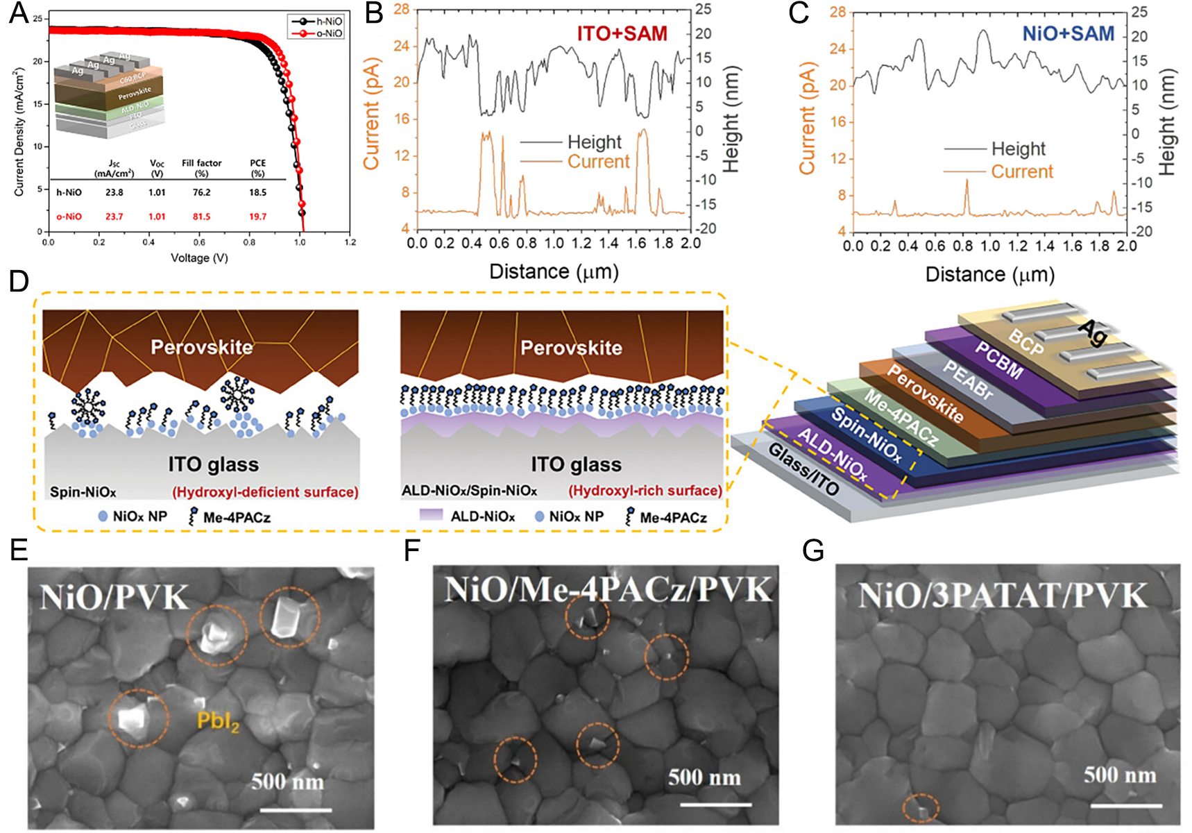
Figure 7. (A) Performance of ALD NiO based PSCs with H2O2(h-)and O3(o-) oxidant[199]. Copyright 2024, Wiley. (B) Current maps from conductive AFM line profiles of SAM and (C) ALD NiO/SAM film[200]. Copyright 2021, American Chemical Society. (D) Illustration of the HTL/perovskite interface and the PSC structure[202]. Copyright 2025, Wiley. (E) SEM images of perovskite films deposited on NiO (F) NiO/MeO-4PACz (G) NiO/3PATAT[203]. Copyright 2025, American Chemical Society.
Device performance of PSCs based on ALD MO HTLs
| Device structure | Product | Precursors | Thickness (nm) | GPC (Å cycle-1) | Temperature (°C) | PCE (%) | Stability | Ref. |
| (Inverted) FTO/ALD NiO/Cs0.05(FA0.95MA0.05)0.90Pb(I0.95Br0.05)3/C60/BCP/Ag | NiO | Ni(dmamb)2, O3 | 7 | 0.3 | 200 | 19.7 | - | [199] |
| (Inverted) ITO/NiO/MeO-2PACz/Cs0.05FA0.92MA0.03Pb(I0.83Br0.17)3/C60/BCP/Ag | NiO | Ni(MeCp)2, O2 plasma | 8 | 0.3 | 150 | 19.0 | AM 1.5G, 85 °C, N2 T75 = 300 h | [200] |
| (Inverted) ITO/NiO/[4-(7H dibenzo[c,g]carbazol-7-yl)butyl]phosphonic Acid (4PADCB) SAM/Cs0.22FA0.78PbI2.55Br0.45/PCBM/BCP/Ag | NiO | Ni(amd)2, H2O | 3.3 | ~0.66 | 160 | 23.3 | AM 1.5G, N2 T84.4 = 1,000 h | [201] |
| (Inverted) ITO/ALD NiO/solution NiO/Me-4PACz/Cs0.05MA0.1FA0.85PbI3/phenethylammonium (PEA)Br/PCBM/BCP/Ag | NiO | Bis(cyclopentadienyl)nickel(II) (Ni(Cp)2), O3 | 2~3 | - | 250 | 25.25 | AM 1.5G, 55 °C, N2 T80 = 600 h | [202] |
| (Inverted) FTO/ALD NiO/3PATAT/(FAPbI3)0.9(CsPbI3)0.05 (MAPbBr3)0.05/C60/BCP/Ag | NiO | Ni(dmamb)2, O3 | - | - | 200 | 25.1 | Dark, RH = 20~30% T92 = 1,000 h | [203] |
| (Inverted) FTO/NiO/Cs0.05MA0.95PbI3/PCBM/BCP/AZO/Ag/Al2O3 | NiO | Ni(dmamb)2, O3 | 20~30 | ~0.25 | 180~230 | 18.8 | - | [207] |
| (Inverted) ITO/ALD NiO/2PACz/Cs0.05FA0.79MA0.16Pb(I0.75Br0.25)3/C60/ALD SnO2/ITO/Ag | NiO | Ni(amd)2, H2O | 8 | ~0.5 | 120 | 16.6 | - | [208] |
| FTO/ALD NiO/(CsPbI3)0.05((FAPbI3)0.95(MAPbBr3)0.05)0.95/C60/BCP/Ag | NiO | - | ~10 | - | 200 | 22.7 | - | [209] |
| ITO/ALD NiO/Cs0.25FA0.75Pb(I0.85Br0.15)3/C60/ALD SnO2/Ag | NiO | Ni(dmamb)2, Cu(dmamb)2, O3 | 8 | - | 120 | 22.47 | 0.8-sun white LED, RH = 40% T95 = 1,000 h | [210] |
ALD MO layer deposition for interface engineering
PSCs face significant interfacial challenges as CTLs improve charge extraction and enhance performance, but interface defects at the CTL/perovskite boundary cause recombination losses[211]. Moreover, CTLs such as spiro-OMeTAD with dopants for improving charge mobilities often exhibit hygroscopicity, accelerating device degradation[212]. To improve both efficiency and stability, interface engineering materials are called for to simultaneously ensure effective charge transport and energy level alignment while maintaining environmental stability[213]. Organic molecules or polymers with functional groups that mediate hydrogen bonds, ionic interactions, or Lewis acid-base coordination can stabilize undercoordinated Pb2+ and halide vacancies at the perovskite surface, reducing interfacial defect density, mitigating Voc losses, and providing an effective passivation strategy[214,215]. Alkylammonium halides such as phenethylammonium iodide (PEAI) and octylammonium bromide (OABr) are also widely applied. Despite their insulating nature which restricts charge transport, the organic spaces form two-dimensional (2D) perovskite more stable against moisture and oxygen than 3D phases[216]. Nonetheless, organic molecules with optimal functionalities require rigorous density functional theory (DFT) calculations and molecular dynamics (MD) simulations for rational design. Alternatively, MOs offer a comparatively established and reliable route, with their synthesis being precisely controllable by ALD[217]. ALD MOs with superior thermal, photochemical, and environmental stability compared to organic counterparts serve as defect-passivating interlayers and protective barriers against ion migration between electrodes and perovskites, improving long-term durability. Chavan et al. modified the mesoporous TiO2 (ms-TiO2) interface with an ultrathin ALD Nb2O5 layer to mitigate charge recombination[218]. Ultraviolet photoelectron spectroscopy (UPS) and UV-vis spectra show that the CB of ms-TiO2 lies at -3.70 eV, slightly above that of the perovskite, thus imposing a ~10 meV barrier to electron transport [Figure 8A]. A 2.1 nm Nb2O5 interlayer lowered the CB to -3.85 eV, resulting in more favorable electron transfer. The Nb2O5 also improved perovskite crystallinity, increased grain size, and smoothed the surface, as confirmed by PL, TRPL, and electrochemical impedance spectroscopy (EIS), which showed reduced nonradiative recombination, accelerated charge extraction, lower series resistance, and higher recombination resistance. Marked improvements were observed, with PCE increasing from 19.1% to 21.0%, hysteresis nearly eliminated, and long-term stability under storage, heat, and UV irradiation significantly enhanced, owing to suppression of oxygen vacancy-mediated O2- formation at the TiO2 interface. Fabricated as an ultrathin ALD layer, Al2O3 reduces nonradiative recombination, blocks moisture and oxygen ingress owing to wide bandgap, optical transparency, and exceptional chemical stability. Zhao et al. investigated the surface chemical evolution of MAPbI3 during Al2O3 ALD using in situ XPS[219]. Upon TMA exposure, the N 1s peak shifted from 402.4 to 401.0 eV, evidencing deprotonation of CH3NH3+ to CH3NH2, which subsequently coordinated with undercoordinated
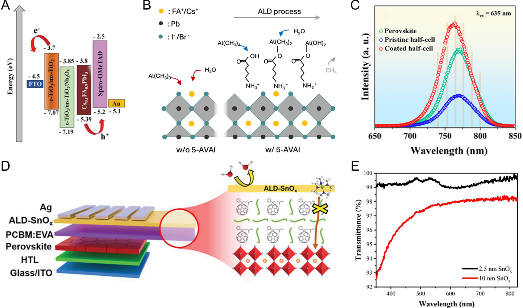
Figure 8. (A) Energy level alignment of regular type PSCs[218]. Copyright 2021, Wiley. (B) Schematic of ALD Al2O3 deposition on perovskite with 5-AVAI[222]. Copyright 2025, Elsevier. (C) ssPL spectra of perovskite film and half-cells with ALD Al2O3 coating[223]. Copyright 2023, American Chemical Society. (D) Schematic illustrating passivation of perovskite/PCBM:EVA film with ALD SnO2[224]. Copyright 2023, Wiley. (E) Transmittance spectra of ALD SnO2 films with different thickness[225]. Copyright 2025, Elsevier.
Device performance of PSCs based on ALD MO interlayers
| Device structure | Product | Precursors | Thickness (nm) | GPC (Å cycle-1) | Temperature (°C) | PCE (%) | Stability | Ref. |
| (Regular) FTO/TiO2/ALD Nb2O5/Cs0.1FA0.9PbI3/spiro-OMeTAD/Au | Nb2O5 | Nb(OEt)5, H2O | 0.7 | 1.4 | 300 | 19.42 | AM 1.5G, RH = 40% T76 = 700 h | [218] |
| (Inverted) FTO/NiO/Al2O3/Cs0.05FA0.79MA0.16PbI3/C60/BCP/Cu | Al2O3 | TMA, H2O | 0.2~0.5 | - | 25 | 22.5 | AM 1.5G, 85 °C, RH = 50% T100 = 2,000 h | [220] |
| (Regular) ITO/SnO2/GA(MA)5Pb5I16/spiro-OMeTAD/Ag | Al2O3 | TMA, H2O | 3 | ~1.0 | 60 | 21.0 | Dark, RH = 40%~50% T93 = 4,080 h | [221] |
| (Inverted) ITO/NiO/Me-4PACz/Cs0.2FA0.8Pb(I0.63Br0.37/5-AVAI/ALD Al2O3/C60/ALD SnO2/Ag | Al2O3 | TMA, H2O | 1.1 | 1.1 | 100 | 19.5 | AM 1.5G, N2 T99 = 615 h | [222] |
| (Regular) FTO/SnO2/(FA0.83MA0.17)0.95Cs0.05PbI2.5Br0.5/spiro-OMeTAD/Au/ALD Al2O3 | Al2O3 | TMA, H2O | - | - | 70 | 20.9 | AM 1.5G, RH = 60% T90 = 300 h | [223] |
| (Inverted) ITO/NiO/PTAA/Al2O3/Cs0.05(FA0.92MA0.08)0.95Pb(I0.92Br0.08)3/PCBM:EVA/ALD SnO2/Ag | SnO2 | TDMASn, H2O | 10 | ~0.5 | 120 | 22.06 | Dark, 85 °C, RH = 85% T85 = 800 h | [224] |
| (Inverted) ITO/MeO-2PACz/Cs0.05FA0.85MA0.10Pb(I0.9Br0.1)3 /C60/BCP/ALD SnO2/Ag | SnO2 | TDMASn, H2O | 2.5 | - | 100 | 17.90 | Dark, RH = 30%~40% T89.6 = 552 h | [225] |
| (Regular) FTO/ALD SnO2/solution SnO2/FAPbI3/spiro-OMeTAD/ALD TiO2/Au | TiO2 | TDMATi, H2O | 4~5 | 0.08~0.10 | 60 | 22.30 | AM 1.5G, 0.85 V bias T96.5 = 120 h | [228] |
| (Inverted) FTO/NiO/MAPbI3/Al2O3/PCBM/Ag | Al2O3 | TMA, H2O | 0.1 | ~0.1 | 75 | 20.4 | AM 1.5G, N2 T95.3 = 3,600 h | [219] |
| (Regular) FTO/c-TiO2/ms-TiO2/FAPbI3/OAI/ALD Al2O3/spiro-OMeTAD/Au | Al2O3 | TMA, H2O | 0.39 | ~0.10 | 100 | 23.75 | AM 1.5G, 85 °C, RH = 85% T90 = 1,872 | [229] |
| (Inverted) FTO/NiO/MeO-4PACz/(FA0.83MA0.17)0.95Cs0.05PbI3/C60/ALD Al2O3/Au | Al2O3 | TMA, H2O | - | - | 20 | 24.61 | AM 1.5G, 65 °C, RH = 30%~50% T90 = 1,150 h | [230] |
| (Inverted) ITO/PTAA/Cs0.05 FA0.70MA0.25PbI2.25Br0.75/PCBM/AZO/ALD SnO2/Ag | SnO2 | TDMASn, H2O | - | - | 100 | 21.50 | AM 1.5G, RH = 30%~40% T84 = 1,000 h | [231] |
| (Inverted) ITO/MeO-4PACz/FA0.7MA0.15Cs0.05Pb(I0.83Br0.17)3/C60/ALD SnO2/Ag | SnO2 | TDMASn, H2O | 15 | 1.2 | 90 | 22.2 | AM 1.5G, 65 °C, N2 T90 = 575 h | [232] |
| (Inverted) FTO/ALD NiO/3PATAT/Cs0.05(FA0.95MA0.05)0.90Pb(I0.95Br0.05)3/C60/ALD SnO2/Ag | SnO2 | TDMASn, H2O | 9~15 | 1.76 | 80~110 | 21.9 | AM 1.5G T91.9 = 2,000 h | [233] |
| (Inverted) ITO/Me-4PACz/Cs0.17FA0.83Pb(I0.80Br0.20)3/Al2O3/C60/ALD SnO2/Ag | SnO2 | TDMASn, H2O | 20 | 1.22 | 80 | 19.26 | - | [234] |
| (Inverted) FTO/Poly[N,N′-bis(4-butylphenyl)-N,N′-bis(phenyl)benzidine] (polyTPD)/MAPbI3/PCBM/ALD SnO2/PEDOT:PSS/Carbon | SnO2 | TDMASn, H2O | - | - | 70 | 16.1 | Real sunlight, -1~36 °C, RH = 40%~80% T94 = 500 h | [235] |
| (Regular) FTO/TiO2/ALD HfAlO/MAPbI3/spiro-OMeTAD/Au | HfAlO | TDMAHf, TMA, H2O | 3 | ~1.0 | 250 | 9.85 | AM 1.5G, RH = 40% T80 = 500 h | [236] |
| (Regular) ITO/SnO2/(FAPbI3)0.85(MAPbBr3)0.15/PTAA/ALD SiAlxOy/ALD SiO2/Au | SiAlxOy, SiO2 | Tetraethyl orthosilicate (TEOS), TMAM, H2O | SiAlxOy:5.2 SiO2:7.3 | SiAlxOy:0.52 SiO2:0.24 | 100 | 19.16 | Dark, RH = 85% T80 = 40 h | [237] |
| (Regular) ITO/SnO2/Cs0.05(FAPbI3)0.85(MAPbBr3)0.15/spiro-OMeTAD/MgO/Au | MgO | MgCp2, H2O | 10.21 | 2 | 80 | 22.74 | Dark, RH = 85% T80 = 162 h | [238] |
CONCLUSION
This review provides an overview of recent progress in ALD MO thin films and offers insights into their application in PSCs. ALD is particularly well-suited to the intrinsic requirements of PSCs, where both high efficiency and long-term stability are demanded. The progress of ALD allows the precise deposition of various MOs, including SnO2 and TiO2 as ETLs, NiO as a HTL, and Al2O3 as an ion diffusion barrier, thereby providing a versatile platform for interface and structural engineering.
Through advances in process design and optimization, ALD MO layers have contributed to remarkable improvements in device performance. Building on the developments, the following subsections highlight the remaining challenges and propose future directions.
Thermal stress-induced degradation
Given that PSCs are constructed from thermally sensitive hybrid materials, the high temperatures typically required in conventional ALD represent a significant limitation. Perovskite absorbers readily decompose or suffer structural degradation above 100 °C, leading to device failure[239]. Thermal stress decomposes the A-site organic cations, and the resulting species subsequently sublime, leaving an excess PbI2. The degradation becomes increasingly severe as the processing time is prolonged. In addition, elevated temperatures can thermally degrade metal precursors, compromising the self-limiting nature of ALD and leading to loss of growth-rate control, non-uniform film formation, and enhanced surface defect generation[240]. Therefore, it is essential to develop appropriate precursors, oxidants, and processing conditions that can produce dense and conductive metal-oxide layers at low temperatures or within short deposition times. The development of precursors and oxidants that can form dense, conductive oxides at reduced temperatures is essential. However, low-temperature deposition often produces amorphous films with poor crystallinity, resulting in inferior charge transport, increased trap density, and elevated interfacial recombination[241,242]. Although PEALD with tailored low-temperature precursor chemistry and post-deposition treatments such as passivation annealing has been investigated to address these issues, shortcomings remain due to plasma-induced substrate damage, film nonuniformity, complex parameter control, and limited large-area uniformity[243,244]. Addressing this challenge to ensure process stability and cost-effectiveness remains critical goals.
Process and precursors compatibility
As interlayers between ETLs or HTLs and perovskite absorbers, ALD MOs facilitate selective charge transport and suppress interfacial recombination. However, strong precursor-perovskite interactions often introduce serious chemical degradation, particularly affecting the organic constituents within hybrid perovskites. Although ALD-derived SnO2 has been widely used as a moisture-blocking protective layer for the top transparent electrodes of tandem and semitransparent PSCs, it was found to induce even faster humidity-driven degradation than bathocuproine (BCP)[230]. During the TDMASn pulse step of the ALD process, the precursor triggers deprotonation of the perovskite A-site organic cations, which accelerates structural collapse under high-temperature and high-humidity conditions. Al2O3, owing to its strong acidic nature, suppresses these degradation pathways and improves long-term stability, yet the TMA precursor can also react with the organic cations and cause lattice disruption and defect formation[245]. Although selecting more suitable precursors and oxidants can mitigate some of these issues, the intrinsic reactivity and thermal stability limitations of ALD restrict the process window to narrow temperature and environmental conditions required for self-limiting growth[55,246]. When interfacial stability is insufficient, device degradation accelerates during long-term operation, with moisture and oxygen further promoting undesirable degradation pathways at the MO/perovskite interface. Consequently, precise optimization of oxide thickness, composition, deposition sequence, and interfacial treatments becomes indispensable. Although ultrathin organic buffer layers inserted prior to ALD can mitigate interfacial reactivity, chemical and structural engineering at the oxide/perovskite boundary still requires substantial refinement[247]. A major challenge in the ALD process for PSC also lies in choosing precursors and oxide materials compatible with the chemical sensitivity of perovskites. Key precursor parameters including volatility, reactivity, stability, and byproduct generation directly determine film quality and process viability[243]. Certain metal precursors exhibit strong reactivity with perovskites, inducing interfacial degradation or unintentional doping[248]. For instance, TiCl4 provides high volatility and rapid deposition kinetics but generates chlorine residues that compromise device performance[249]. Metal-organic Ti precursors yield films of higher purity, a characteristic offset by their low volatility, which often requires elevated deposition temperatures[250]. The structural and chemical properties of the deposited MO is determined by precursor selection, and this directly affects the electronic and optical characteristics[251]. Accordingly, the composition engineering of MO layers determines a decisive influence on optical transparency, electron affinity, and band alignment. Insufficient energy-level alignment of the deposited materials leads to charge transport barriers and consequently lowers efficiency[252]. Consequently, establishing an optimal combination of precursor chemistry and oxide material is essential to balance film purity, electronic and optical functionality, and interfacial stability.
Toward commercialization
Despite the precision and controllability of ALD, the slow cycle-by-cycle growth kinetics imposes severe limitations on scalability. For PSC modules, MO films must be deposited uniformly over substrates extending to several tens of square centimeters, but the inherently low growth rate of ALD significantly limits manufacturing throughput[253]. Moreover, when micrometer-scale MO layers are required in PV modules, the process becomes impractically time-consuming as ALD struggles to achieve even film thicknesses beyond a few tens of nanometers within reasonable durations[254]. High equipment costs and long cycle durations further escalate production expenses. PEALD enables the deposition of MO films at low temperatures with high uniformity and smooth surfaces, making it suitable for application in PSCs. However, an excessively long precursor pulse time can induce unintended CVD reactions during the process, thereby compromising film uniformity and process controllability. Insufficient plasma exposure time, which must be carefully optimized for process throughput and efficiency, can also lead to reduced GPC, nonuniform film thickness, and degraded film quality[255]. Highly reactive radicals cause substrate defects, complicating process control and limiting the reproducibility of low damage conditions at large scale[256]. While SALD, roll-to-roll integration, and hybrid deposition schemes have been proposed to accelerate processes, persistent trade-offs among uniformity, throughput, and cost remain unresolved[257,258]. In the SALD process, all precursors are introduced simultaneously into spatially separated reaction zones that are divided by physical or gaseous barriers. However, undesired gas mixing between these zones may still occur. Increasing the process temperature to accelerate reaction kinetics can lead to precursor decomposition and particle sintering, while lowering the temperature often results in incomplete adsorption and condensation of precursors[259]. These trade-offs hinder the formation of uniform and conformal films. Therefore, although the implementation of SALD enables higher throughput and continuous operation for industrial-scale production, it inherently faces structural bottlenecks that limit film uniformity and process scalability. Achieving scalable, high-productivity ALD processes thus continues to be a major hurdle for industrial deployment.
Summary and outlook
ALD MOs represent a promising route to advancing material quality and interfacial control in PSCs. Although ALD does not yet fully surpass the simplicity and throughput of solution processing, it stands out as the most effective strategy for introducing protective buffer and encapsulation layers that enhance stability. Future progress will require the development of low-temperature precursors and processes, improved interfacial stabilization strategies, and scalable large-area manufacturing technologies. With these advancements, ALD is poised to play a decisive role in achieving both high efficiency and durability in PSCs. Ultimately, bridging the gap between academic research and industrial application through close collaboration will be pivotal in accelerating the path to commercialization of ALD. Such integrative progress is expected to drive the practical deployment of next-generation photovoltaics and contribute significantly to sustainable energy transition.
DECLARATIONS
Authors’ contributions
Writing original manuscript, reviewing and editing: Park, P. J.
Reviewing and editing: Jo, H. J.; Han, S. M.; Kim, Y. J.; Kim, S. Y.
Availability of data and materials
Not applicable.
AI and AI-assisted tools statement
Not applicable.
Financial support and sponsorship
This research was supported in part by the NRF funded by the Korean government [RS-2025-00558945] and in part by Korea Institute of Marine Science & Technology Promotion (KIMST) funded by the Ministry of Oceans and Fisheries (RS-2024-00406639)
Conflicts of interest
All authors declared that there are no conflicts of interest.
Ethical approval and consent to participate
Not applicable.
Consent for publication
Not applicable.
Copyright
© The Author(s) 2026.
REFERENCES
1. Zhong, K.; Sun, P.; Xu, H. Advances in defect engineering of metal oxides for photocatalytic CO2 reduction. Small 2025, 21, 2310677.
2. Kim, J. H.; Kim, J.; Ma, J.; et al. Spontaneous metal-chelation strategy for highly dense Ni single-atom catalysts with asymmetric coordination in CO2 electroreduction. Small 2025, 21, 2409481.
3. Ma, J.; Lee, W.; Kim, J. H.; et al. Leveraging the intermetal distance in dual-atom catalysts: revealing optimized synergistic interactions for CO2 electroreduction. ACS. Nano. 2025, 19, 18698-707.
4. Oni, A. M.; Mohsin, A. S.; Rahman, M. M.; Bhuian, M. B. H. A comprehensive evaluation of solar cell technologies, associated loss mechanisms, and efficiency enhancement strategies for photovoltaic cells. Energy. Rep. 2024, 11, 3345-66.
5. Jang, W. J.; Park, P. J.; Ma, J.; Kim, S. Y. Engineering perovskite solar cells for photovoltaic and photoelectrochemical systems: strategies for enhancing efficiency and stability. Chem. Commun. 2025, 61, 8137-56.
6. Sabatino M, Hendawi R, Garcia AS. Silicon solar cells: trends, manufacturing challenges, and AI perspectives. Crystals 2024, 14, 167.
7. Khokhar, M. Q.; Yousuf, H.; Jeong, S.; et al. A review on p-type tunnel oxide passivated contact (TOPCon) solar cell. Trans. Electr. Electron. Mater. 2023, 24, 169-77.
8. Rehman, Z. U.; Lin, Z. Inorganic M3ACl3 (M=Ca, Sr, Ba, A=N, P, As) perovskite-derivatives for next-generation solar cells and optoelectronics: in-depth analysis of stability, optoelectronic features, and temperature-dependent carrier mobilities. J. Mater. Chem. A. 2025, 13, 34469-92.
9. Wang, J.; Feng, Y.; He, Y. Advancements in recycling technologies for waste CIGS photovoltaic modules. Nano. Energy. 2024, 128, 109847.
10. Camargo, P. S. S.; Petroli, P. A.; de, Souza. R. A.; et al. CdTe photovoltaic technology: an overview of waste generation, recycling, and raw material demand. Curr. Opin. Green. Sustain. Chem. 2024, 47, 100904.
11. Shah, U. A.; Wang, A.; Irfan, Ullah. M.; et al. A deep dive into Cu2ZnSnS4 (CZTS) solar cells: a review of exploring roadblocks, breakthroughs, and shaping the future. Small 2024, 20, 2310584.
12. Mahboob, S.; Rizwana,
13. Hedibi, A.; Gueddim, A.; Bentria, B. Numerical modeling and optimization of ZnO: Al/iZnO/ZnMgO/CZTS photovoltaic solar cell. Trans. Electr. Electron. Mater. 2021, 22, 666-72.
14. Zyoud, S. H.; Zyoud, A. H.; Ahmed, N. M.; Abdelkader, A. F. Numerical modelling analysis for carrier concentration level optimization of CdTe heterojunction thin film-based solar cell with different non-toxic metal chalcogenide buffer layers replacements: using SCAPS-1D software. Crystals 2021, 11, 1454.
15. Yi, J.; Zhang, G.; Yu, H.; Yan, H. Advantages, challenges and molecular design of different material types used in organic solar cells. Nat. Rev. Mater. 2024, 9, 46-62.
16. Ding, P.; Yang, D.; Yang, S.; Ge, Z. Stability of organic solar cells: toward commercial applications. Chem. Soc. Rev. 2024, 53, 2350-87.
17. Lee, J. W.; Park, J. S.; Jeon, H.; et al. Recent progress and prospects of dimer and multimer acceptors for efficient and stable polymer solar cells. Chem. Soc. Rev. 2024, 53, 4674-706.
18. Sorrentino, R.; Kozma, E.; Luzzati, S.; Po, R. Interlayers for non-fullerene based polymer solar cells: distinctive features and challenges. Energy. Environ. Sci. 2021, 14, 180-223.
19. Kojima, A.; Teshima, K.; Shirai, Y.; Miyasaka, T. Organometal halide perovskites as visible-light sensitizers for photovoltaic cells. J. Am. Chem. Soc. 2009, 131, 6050-1.
20. Zhang, X.; Wu, S.; Zhang, H.; et al. Advances in inverted perovskite solar cells. Nat. Photonics. 2024, 18, 1243-53.
21. Wu, T.; Qin, Z.; Wang, Y.; et al. The main progress of perovskite solar cells in 2020-2021. Nano. Micro. Lett. 2021, 13, 152.
22. Kothandaraman, R. K.; Jiang, Y.; Feurer, T.; et al. Near-infrared-transparent perovskite solar cells and perovskite-based tandem photovoltaics. Small. Methods. 2020, 4, 2000395.
23. Wang, S.; Wang, A.; Hao, F. Toward stable lead halide perovskite solar cells: a knob on the A/X sites components. iScience 2022, 25, 103599.
24. Miah, M. H.; Khandaker, M. U.; Rahman, M. B.; et al. Band gap tuning of perovskite solar cells for enhancing the efficiency and stability: issues and prospects. RSC. Adv. 2024, 14, 15876-906.
25. Han, J.; Park, K.; Tan, S.; et al. Perovskite solar cells. Nat. Rev. Methods. Primers. 2025, 5, 3.
26. Green, M. A.; Dunlop, E. D.; Yoshita, M.; et al. Solar cell efficiency tables (version 64). Prog. Photovolt. Res. Appl. 2024, 32, 425-41.
27. Aydin, E.; Allen, T. G.; De, Bastiani. M.; et al. Pathways toward commercial perovskite/silicon tandem photovoltaics. Science 2024, 383, eadh3849.
28. Yang, G.; Deng, C.; Li, C.; et al. Towards efficient, scalable and stable perovskite/silicon tandem solar cells. Nat. Photonics. 2025, 19, 913-24.
29. Chao, L.; Niu, T.; Gao, W.; et al. Solvent engineering of the precursor solution toward large-area production of perovskite solar cells. Adv. Mater. 2021, 33, 2005410.
30. Yang, F.; Jang, D.; Dong, L.; et al. Upscaling solution-processed perovskite photovoltaics. Adv. Energy. Mater. 2021, 11, 2101973.
31. Wang, C.; Nie, R.; Dai, Y.; et al. Enhancing the inherent stability of perovskite solar cells through chalcogenide-halide combinations. Energy. Environ. Sci. 2024, 17, 1368-86.
32. Kore, B. P.; Jamshidi, M.; Gardner, J. M. The impact of moisture on the stability and degradation of perovskites in solar cells. Mater. Adv. 2024, 5, 2200-17.
33. Mesquita, I.; Andrade, L.; Mendes, A. Effect of relative humidity during the preparation of perovskite solar cells: performance and stability. Sol. Energy. 2020, 199, 474-83.
34. Huang, P. C.; Yang, T. J.; Lin, C. J.; et al. Unraveling the heat- and UV-induced degradation of mixed halide perovskite thin films via surface analysis techniques. Langmuir 2024, 40, 11873-87.
35. Song, J.; Liu, H.; Pu, W.; et al. Thermal instability originating from the interface between organic-inorganic hybrid perovskites and oxide electron transport layers. Energy. Environ. Sci. 2022, 15, 4836-49.
36. Tang, J.; Tian, W.; Zhao, C.; et al. Imaging the moisture-induced degradation process of 2D organolead halide perovskites. ACS. Omega. 2022, 7, 10365-71.
37. Ma, H.; Ahn, E.; Lee, D.; et al. Water-induced degradation mechanism of metal halide perovskite nanocrystals. Matter 2025, 8, 102083.
38. Zhou, P.; Liu, Q.; Zhang, Z. Coupled modeling of solvent evaporation and thin film evolution in spin coating. Appl. Therm. Eng. 2025, 279, 127662.
39. Sin, J.; Kim, H.; Kim, M.; et al. Anti-solvent treatment time approach to high efficiency perovskite solar cells with temperature of coating environmental. Sol. Energy. Mater. Sol. Cells. 2023, 250, 112054.
40. Wang, T.; Zhang, T.; Zhang, J.; et al. Additive-regulated one-step dynamic spin-coating for fabricating high-performance perovskite solar cells under high humidity conditions. J. Mater. Chem. C. 2024, 12, 913-21.
41. Al-Katrib, M.; Perrin, L.; Flandin, L.; Planes, E. Electrodeposition in perovskite solar cells: a critical review, new insights, and promising paths to future industrial applications. Adv. Mater. Technol. 2023, 8, 2300964.
42. Njema, G. G.; Kibet, J. K.; Ngari, S. M. A review of interface engineering characteristics for high performance perovskite solar cells. Measurement. Energy. 2024, 2, 100005.
43. Jang, W. J.; Kim, E. H.; Cho, J. H.; et al. Elucidating the role of alkali metal carbonates in impact on oxygen vacancies for efficient and stable perovskite solar cells. Adv. Sci. 2024, 11, 2406657.
44. Cao, Y.; Yan, N.; Wang, M.; et al. Designed additive to regulated crystallization for high performance perovskite solar cell. Angew. Chem. Int. Ed. 2024, 63, e202404401.
45. Azam, M.; Ke, Z.; Luo, J.; et al. Additive engineering enabled non-radiative defect passivation with improved moisture-resistance in efficient and stable perovskite solar cells. Chem. Eng. J. 2024, 483, 149424.
46. He, Z.; Peng, C.; Guo, R.; et al. High-efficiency and emission-tunable inorganic blue perovskite light-emitting diodes based on vacuum deposition. Small 2024, 20, 2305379.
47. Liu, L.; Yang, S. E.; Liu, P.; Chen, Y. High-quality and full-coverage CsPbBr3 thin films via electron beam evaporation with post-annealing treatment for all-inorganic perovskite solar cells. Sol. Energy. 2022, 232, 320-7.
48. Xu, Z.; Chin, S. H.; Park, B. I.; et al. Advancing perovskite solar cell commercialization: bridging materials, vacuum deposition, and AI-assisted automation. Next. Mater. 2024, 3, 100103.
49. Zhou, C.; Meng, W.; Kong, L.; et al. Vacuum processed metal halide perovskite light-emitting diodes. Adv. Funct. Mater. 2024, 34, 2307682.
50. Tong, G.; Zhang, J.; Bu, T.; et al. Holistic strategies lead to enhanced efficiency and stability of hybrid chemical vapor deposition based perovskite solar cells and modules. Adv. Energy. Mater. 2023, 13, 2300153.
51. Lee, J. H.; Kim, B. S.; Park, J.; et al. Opportunities and challenges for perovskite solar cells based on vacuum thermal evaporation. Adv. Mater. Technol. 2023, 8, 2200928.
52. Soto-Montero, T.; Kralj, S.; Azmi, R.; et al. Single-source pulsed laser-deposited perovskite solar cells with enhanced performance via bulk and 2D passivation. Joule 2024, 8, 3412-25.
53. Zhao, R.; Mao, P.; Lv, J.; et al. Atomic layer deposition processed interlayers in photovoltaics: applications, challenges and perspectives. J. Energy. Chem. 2025, 109, 702-25.
54. Asare, G. K.; Adu, J. S.; Shin, B.; et al. Perspective: atomic layer deposition strategies for surface passivation of metal-halide perovskite absorbers. Electron. Mater. Lett. 2025, 21, 331-6.
55. Zhang, J.; Li, Y.; Cao, K.; Chen, R. Advances in atomic layer deposition. Nanomanuf. Metrol. 2022, 5, 191-208.
56. Yasmeen, S.; Ryu, S. W.; Lee, S. H.; Lee, H. B. R. Atomic layer deposition beyond thin film deposition technology. Adv. Mater. Technol. 2023, 8, 2200876.
57. Tran, V. H. A.; Lims, S. C.; Anwar, N.; et al. Atomic layer deposition of metal and metal oxides: mechanisms, challenges, and future prospects. J. Alloys. Compd. 2025, 1041, 183864.
58. Park, H. H.; Fermin, D. J. Recent developments in atomic layer deposition of functional overlayers in perovskite solar cells. Nanomaterials 2023, 13, 3112.
59. Menon, V. S.; Krishnamoorthy, A. Hole selectivity of n-type molybdenum oxide carrier selective layer for commercial and emerging thin-film photovoltaics: a critical analysis of interface energetics and ensuant device physics. Energy. Technol. 2023, 11, 2300608.
60. Zhang, C.; Pei, K.; Sheng, T.; et al. Metal oxides engineering: toward sustainable superhydrophobic surfaces. Adv. Funct. Mater. 2025, 36, e12239.
61. Sambathkumar, C.; Nagavenkatesh, K.; Thangavel, R.; et al. Investigation and comparative studies on charge storage performance in nanostructured RuO2, NiO and Co3O4 nanoparticles for high dense energy storage. Electron. Mater. Lett. 2024, 20, 571-83.
62. Singh, R.; Ghosh, S.; Subbiah, A. S.; et al. ALD Al2O3 on hybrid perovskite solar cells: unveiling the growth mechanism and long-term stability. Sol. Energy. Mater. Sol. Cells. 2020, 205, 110289.
63. Liu, Y.; Sang, B.; Hossain, M. A.; et al. A novel passivating electron contact for high-performance silicon solar cells by ALD Al-doped TiO2. Sol. Energy. 2021, 228, 531-9.
64. Di, Mario. L.; Garcia, Romero. D.; Wang, H.; et al. Outstanding fill factor in inverted organic solar cells with SnO2 by atomic layer deposition. Adv. Mater. 2024, 36, 2301404.
65. Kim, H. M.; Kim, D. G.; Kim, Y. S.; et al. Atomic layer deposition for nanoscale oxide semiconductor thin film transistors: review and outlook. Int. J. Extreme. Manuf. 2023, 5, 012006.
66. Gurbandurdyyev, G.; Mistry, K.; Delumeau, L. V.; et al. Robust, conformal ZnO coatings on fabrics via atmospheric-pressure spatial atomic layer deposition with in-situ thickness control. ChemNanoMat 2023, 9, e202200498.
67. Li, B.; Härtel, M.; Al-Ashouri, A.; et al. Atomic-layer-deposition-free monolithic perovskite/silicon tandem solar cell reaching 29.91% power conversion on industrial PERX/TOPCon-like silicon bottom cells. ACS. Energy. Lett. 2024, 9, 4550-6.
68. Lee, S. U.; Kim, S. Y.; Lee, J. H.; et al. Artificial synapse based on a δ-FAPbI3/atomic-layer-deposited SnO2 bilayer memristor. Nano. Lett. 2024, 24, 4869-76.
69. Li, R.; Li, N.; Hou, J.; et al. Aquatic environment remediation by atomic layer deposition-based multi-functional materials: a review. J. Hazard. Mater. 2021, 402, 123513.
70. Richey, N. E.; de, Paula. C.; Bent, S. F. Understanding chemical and physical mechanisms in atomic layer deposition. J. Chem. Phys. 2020, 152, 040902.
71. Jan, A.; Tanis-Kanbur, M. B.; Rietveld, L. C.; Heijman, S. G. J. A review on atomically modified materials by atomic layer deposition for wastewater treatment. Open. Ceram. 2025, 22, 100780.
72. Yarbrough, J.; Shearer, A. B.; Bent, S. F. Next generation nanopatterning using small molecule inhibitors for area-selective atomic layer deposition. J. Vac. Sci. Technol. A. 2021, 39, 021002.
73. Paek, S.; Schouwink, P.; Athanasopoulou, E. N.; et al. From nano- to micrometer scale: the role of antisolvent treatment on high performance perovskite solar cells. Chem. Mater. 2017, 29, 3490-8.
74. Ma, Y.; Liu, C.; Zhang, M.; Mai, Y. Review on the effects of solvent physical properties on the performance of slot-die coated perovskite solar cells. Surf. Sci. Technol. 2024, 2, 25.
75. Taylor, A. D.; Sun, Q.; Goetz, K. P.; et al. A general approach to high-efficiency perovskite solar cells by any antisolvent. Nat. Commun. 2021, 12, 1878.
76. Nattoo, C. A.; Peña, T.; Nassiri, Nazif. K.; et al. Optoelectronic properties of atomic layer deposited and sputtered MoS2 films. ACS. Appl. Mater. Interfaces. 2025, 17, 47347-54.
77. Zhao, W.; Duan, Y. Advanced applications of atomic layer deposition in perovskite-based solar cells. Adv. Photonics. Res. 2021, 2, 2100011.
78. Armstrong, C.; Delumeau, L. V.; Muñoz-Rojas, D.; et al. Tuning the band gap and carrier concentration of titania films grown by spatial atomic layer deposition: a precursor comparison. Nanoscale. Adv. 2021, 3, 5908-18.
79. Dutta, T.; Yadav, N.; Wu, Y.; et al. Electronic properties of 2D materials and their junctions. Nano. Mater. Sci. 2024, 6, 1-23.
80. Nguyen, C. T.; Cho, E. H.; Gu, B.; et al. Gradient area-selective deposition for seamless gap-filling in 3D nanostructures through surface chemical reactivity control. Nat. Commun. 2022, 13, 7597.
81. Choi, D. W.; Maeng, W. J.; Park, J. S. The conducting tin oxide thin films deposited via atomic layer deposition using tetrakis-dimethylamino tin and peroxide for transparent flexible electronics. Appl. Surf. Sci. 2014, 313, 585-90.
82. Qiu, S.; Amaro, A.; Fabulyak, D.; et al. Impact of tetrakis(dimethylamido)tin(IV) degradation on atomic layer deposition of tin oxide films and perovskite solar cells. Small 2025, 21, 2404966.
83. Sheng, J.; Han, K. L.; Hong, T.; et al. Review of recent progresses on flexible oxide semiconductor thin film transistors based on atomic layer deposition processes. J. Semicond. 2018, 39, 011008.
84. Hong, T.; Kim, H. W.; Kim, Y. S.; et al. Plasma-enhanced atomic layer deposition assisted low-temperature synthetic routes to rationally designed metastable C-axis aligned hexagonal In-Zn-O. Chem. Mater. 2023, 35, 5168-76.
85. Lee, S.; Kim, M.; Mun, G.; et al. Effects of Al precursors on the characteristics of indium-aluminum oxide semiconductor grown by plasma-enhanced atomic layer deposition. ACS. Appl. Mater. Interfaces. 2021, 13, 40134-44.
86. Wang, C.; Zhao, D.; Grice, C. R.; et al. Low-temperature plasma-enhanced atomic layer deposition of tin oxide electron selective layers for highly efficient planar perovskite solar cells. J. Mater. Chem. A. 2016, 4, 12080-7.
87. Wang, H.; Zhao, Y.; Wang, Z.; et al. Hermetic seal for perovskite solar cells: an improved plasma enhanced atomic layer deposition encapsulation. Nano. Energy. 2020, 69, 104375.
88. Preischel, F.; Zanders, D.; Berning, T.; et al. Interplay of precursor and plasma for the deposition of HfO2 via PEALD: film growth and dielectric properties. Adv. Mater. Interfaces. 2023, 10, 2300244.
89. Xu, L.; Zhang, Z.; Yang, L.; Yang, J.; Wang, P.; Gao, G.; et al. Comparison of thermal, plasma-enhanced and layer by layer Ar plasma treatment atomic layer deposition of tin oxide thin films. J. Cryst. Growth. 2021, 572, 126264.
90. Oviroh, P. O.; Akbarzadeh, R.; Pan, D.; Coetzee, R. A. M.; Jen, T. C. New development of atomic layer deposition: processes, methods and applications. Sci. Technol. Adv. Mater. 2019, 20, 465-96.
91. Sønsteby, H. H.; Yanguas-Gil, A.; Elam, J. W. Consistency and reproducibility in atomic layer deposition. J. Vac. Sci. Technol. A. 2020, 38, 020804.
92. Poodt, P.; Cameron, D. C.; Dickey, E.; et al. Spatial atomic layer deposition: a route towards further industrialization of atomic layer deposition. J. Vac. Sci. Technol. A. 2012, 30, 010802.
93. Asgarimoghaddam, H.; Chen, Q.; Ye, F.; Shahin, A.; Song, B.; Musselman, K. P. Zinc aluminum oxide encapsulation layers for perovskite solar cells deposited using spatial atomic layer deposition. Small. Methods. 2024, 8, 2300995.
94. Yersak, A. S.; Sharma, K.; Wallas, J. M.; Dameron, A. A.; Li, X.; Yang, Y.; et al. Spatial atomic layer deposition for coating flexible porous Li-ion battery electrodes. J. Vac. Sci. Technol. A. 2018, 36, 01A123.
95. Muñoz-Rojas, D.; MacManus-Driscoll, J. Spatial atmospheric atomic layer deposition: a new laboratory and industrial tool for low-cost photovoltaics. Mater. Horiz. 2014, 1, 314-20.
96. Vale, J. P.; Sekkat, A.; Gheorghin, T.; et al. Can we rationally design and operate spatial atomic layer deposition systems for steering the growth regime of thin films? J. Phys. Chem. C. 2023, 127, 9425-36.
97. Jiang, X.; Shan, B.; Ma, G.; et al. Scalable deposition of SnO2 ETL via SALD for large-area inverted perovskite solar modules. Chem. Eng. J. 2025, 505, 159629.
98. Qian, J.; Xu, B.; Tian, W. A comprehensive theoretical study of halide perovskites ABX3. Org. Electron. 2016, 37, 61-73.
99. Li, C.; Lu, X.; Ding, W.; Feng, L.; Gao, Y.; Guo, Z. Formability of ABX3 (X = F, Cl, Br, I) halide perovskites. Acta. Cryst. B. Struct. Sci. 2008, 64, 702-7.
100. Sato, T.; Takagi, S.; Deledda, S.; Hauback, B. C.; Orimo, S. I. Extending the applicability of the Goldschmidt tolerance factor to arbitrary ionic compounds. Sci. Rep. 2016, 6, 23592.
101. Teo, S. H.; Ng, C. H.; Ng, Y. H.; Islam, A.; Hayase, S.; Taufiq-Yap, Y. H. Resolve deep-rooted challenges of halide perovskite for sustainable energy development and environmental remediation. Nano. Energy. 2022, 99, 107401.
102. Meloni, S.; Palermo, G.; Ashari-Astani, N.; Grätzel, M.; Rothlisberger, U. Valence and conduction band tuning in halide perovskites for solar cell applications. J. Mater. Chem. A. 2016, 4, 15997-6002.
103. Kusuma, F. J.; Widianto, E.; Wahyono,
104. Ko, P. K.; Ge, J.; Ding, P.; et al. The deepest blue: major advances and challenges in deep blue emitting quasi-2D and nanocrystalline perovskite LEDs. Adv. Mater. 2025, 37, 2407764.
105. Ji, L.; Zhang, X.; Zhang, T.; et al. Band alignment of Pb-Sn mixed triple cation perovskites for inverted solar cells with negligible hysteresis. J. Mater. Chem. A. 2019, 7, 9154-62.
106. Chen, L.; Yoo, J. W.; Hu, M.; Lee, S. U.; Seok, S. I. Intrinsic phase stability and inherent bandgap of formamidinium lead triiodide perovskite single crystals. Angew. Chem. Int. Ed. 2022, 61, e202212700.
107. Kaiser, W.; Hussain, K.; Singh, A.; et al. Defect formation and healing at grain boundaries in lead-halide perovskites. J. Mater. Chem. A. 2022, 10, 24854-65.
108. Guo, Z.; Wang, J.; Yin, W. J. Atomistic origin of lattice softness and its impact on structural and carrier dynamics in three dimensional perovskites. Energy. Environ. Sci. 2022, 15, 660-71.
109. Liu, Y.; Lv, W.; Feng, J.; et al. Emerging thermochromic perovskite materials: insights into fundamentals, recent advances and applications. Adv. Funct. Mater. 2024, 34, 2402234.
110. Wang, F.; Bai, S.; Tress, W.; Hagfeldt, A.; Gao, F. Defects engineering for high-performance perovskite solar cells. NPJ. Flex. Electron. 2018, 2, 22.
111. Baumann, F.; Raga, S. R.; Lira-Cantú, M. Monitoring the stability and degradation mechanisms of perovskite solar cells by in situ and operando characterization. APL. Energy. 2023, 1, 011501.
112. Wąsiak-Maciejak, A.; Przypis, Ł.; Żuraw, W.; et al. Compositional and interfacial engineering for improved light stability of flexible wide-bandgap perovskite solar cells. J. Mater. Chem. A. 2025, 13, 7335-46.
113. Wang, H.; Zhang, Z.; Wang, X.; Duan, L.; Luo, J. Phenyltrimethylammonium chloride additive for highly efficient and stable FAPbI3 perovskite solar cells. Nano. Energy. 2024, 123, 109423.
114. Heo, D. Y.; Jang, W. J.; Jeong, M. J.; Noh, J. H.; Kim, S. Y. Optimal solvents for interfacial solution engineering of perovskite solar cells. Sol. RRL. 2022, 6, 2200485.
115. Xu, C.; Hang, P.; Kan, C.; Guo, X.; Song, X.; Xu, C.; et al. Molecular ferroelectric self-assembled interlayer for efficient perovskite solar cells. Nat. Commun. 2025, 16, 835.
116. Li, S.; Li, X.; Dai, C.; He, W.; Shabdan, Y.; Guli, M. Research on the application of metal oxide buffer layers in perovskite solar cells. Chem. Eng. J. 2025, 521, 166935.
117. Park, H.; Jeong, S.; Kim, E.; Shin, S.; Shin, H. Hole-transporting vanadium-containing oxide (V2O5-x) interlayers enhance stability of α-FAPbI3-based perovskite solar cells (~23%). ACS. Appl. Mater. Interfaces. 2022, 14, 42007-17.
118. Dong, J.; Jia, J.; Shi, B.; Feng, X.; Wu, Y.; Lv, P.; et al. Cr2O3 interlayer at TiO2/perovskite interface propelling the efficiency improvement of perovskite solar cells. Surf. Interfaces. 2022, 29, 101761.
119. Li, H.; Gao, B.; Yang, L.; et al. Magnesium oxide buffer layer for over 32% efficiency four-terminal perovskite/silicon tandem solar cells. Adv. Energy. Mater. 2025, 15, 2501762.
120. Moumen, A.; Kumarage, G. C.; Comini, E. P-type metal oxide semiconductor thin films: synthesis and chemical sensor applications. Sensors 2022, 22, 1359.
121. Valadi, K.; Gharibi, S.; Taheri-Ledari, R.; Akin, S.; Maleki, A.; Shalan, A. E. Metal oxide electron transport materials for perovskite solar cells: a review. Environ. Chem. Lett. 2021, 19, 2185-207.
122. Zhou, G.; Luo, X.; Wang, Z.; et al. Recent progress on cross-linkable fullerene-based electron transport materials for perovskite solar cells. ChemSusChem 2025, 18, e202401629.
123. Kim, K.; Kim, M.; Lee, H.; Chung, D. W.; Kim, J. Multi-functional PEDOT:PSS as the efficient perovskite solar cells. Small 2024, 20, 2402341.
124. Arumugam, G. M.; Karunakaran, S. K.; Liu, C.; et al. Inorganic hole transport layers in inverted perovskite solar cells: a review. Nano. Select. 2021, 2, 1081-116.
125. Murugan, P.; Hu, T.; Hu, X.; Chen, Y. Advancements in organic small molecule hole-transporting materials for perovskite solar cells: past and future. J. Mater. Chem. A. 2022, 10, 5044-81.
126. Althumayri, M.; Das, R.; Banavath, R.; Beker, L.; Achim, A. M.; Ceylan, Koydemir. H. Recent advances in transparent electrodes and their multimodal sensing applications. Adv. Sci. 2024, 11, 2405099.
127. Wang, C.; Li, J.; Luo, C.; et al. SnO2-based resistive hydrogen gas sensor: a comprehensive review from performance to function optimization. Mater. Sci. Semicond. Process. 2025, 188, 109209.
128. Phogat, P.; Jha, R.; Singh, S. Harnessing ZnO morphologies in energy application and sustainable development. Phys. Scr. 2024, 99, 102004.
129. Chen, K. T.; Hsu, C. H.; Ren, F. B.; et al. Influence of annealing temperature of nickel oxide as hole transport layer applied for inverted perovskite solar cells. J. Vac. Sci. Technol. A. 2021, 39, 062401.
130. Patel, V. D.; Gupta, D. Solution-processed metal-oxide based hole transport layers for organic and perovskite solar cell: a review. Mater. Today. Commun. 2022, 31, 103664.
131. Wu, S.; Liu, M.; Jen, A. K. Y. Prospects and challenges for perovskite-organic tandem solar cells. Joule 2023, 7, 484-502.
132. Szabó, G.; Kamat, P. V. Spiro-OMeTAD: unique redox chemistry driving the hole transport. ACS. Energy. Lett. 2024, 10, 330-6.
133. Duan, Y.; Chen, Y.; Wu, Y.; Liu, Z.; Liu, S.; Peng, Q. A comprehensive review of organic hole-transporting materials for highly efficient and stable inverted perovskite solar cells. Adv. Funct. Mater. 2024, 34, 2315604.
134. Ouedraogo, N. A. N.; Odunmbaku, G. O.; Guo, B.; et al. Oxidation of spiro-OMeTAD in high-efficiency perovskite solar cells. ACS. Appl. Mater. Interfaces. 2022, 14, 34303-27.
135. Ahmad, N.; Yuan, J.; Zou, Y. One more step towards better stability of non-fullerene organic solar cells: advances, challenges, future perspectives, and the era of artificial intelligence. Energy. Environ. Sci. 2025, 18, 5093-158.
136. Kim, S.; Lee, S. H.; Jo, I. H.; Park, T. J.; Kim, J. H. Reduced leakage current in atomic-layer-deposited HfO2 thin films deposited at low temperature by in situ defect passivation. Appl. Surf. Sci. 2024, 645, 158790.
137. Yao, Q.; Song, H.; Zhang, M.; et al. Recent advances in semi-transparent perovskite solar cells: fabrication, structural engineering, applications, and future challenges. J. Mater. Chem. C. 2025, 13, 22059-103.
138. Chen, R.; Zhang, W.; Guan, X.; et al. Rear electrode materials for perovskite solar cells. Adv. Funct. Mater. 2022, 32, 2200651.
139. Brinkmann, K. O.; Gahlmann, T.; Riedl, T. Atomic layer deposition of functional layers in planar perovskite solar cells. Sol. RRL. 2020, 4, 1900332.
140. Kim, B. J.; Jang, J. H.; Kim, J.; Oh, K. S.; Choi, E. Y.; Park, N. Efficiency and stability enhancement of organic–inorganic perovskite solar cells through micropatterned Norland optical adhesive and polyethylene terephthalate encapsulation. Mater. Today. Commun. 2019, 20, 100537.
141. Wang, Y.; Ahmad, I.; Leung, T.; et al. Encapsulation and stability testing of perovskite solar cells for real life applications. ACS. Mater. Au. 2022, 2, 215-36.
142. Lv, Y.; Xu, P.; Ren, G.; et al. Low-temperature atomic layer deposition of metal oxide layers for perovskite solar cells with high efficiency and stability under harsh environmental conditions. ACS. Appl. Mater. Interfaces. 2018, 10, 23928-37.
143. Allen, O. J.; Kang, J.; Qian, S.; Hinsch, J. J.; Zhang, L.; Wang, Y. A theoretical review of passivation technologies in perovskite solar cells. Energy. Mater. 2024, 4, 400037.
144. Lin, L.; Jones, T. W.; Yang, T. C. J.; et al. Hydrogen bonding in perovskite solar cells. Matter 2024, 7, 38-58.
145. Walsh, A.; Yan, Y.; Huda, M. N.; Al-Jassim, M. M.; Wei, S. H. Band edge electronic structure of BiVO4: elucidating the role of the Bi s and V d orbitals. Chem. Mater. 2009, 21, 547-51.
146. Wang, Y.; Ba, Z.; Dong, S.; Xie, W.; Wu, Z.; Ran, C. Advancing SnO2 electron transport layer for efficient perovskite photovoltaics: a critical review. ACS. Appl. Mater. Interfaces. 2025, 17, 27651-70.
147. Bae, D.; Kwon, S.; Oh, J.; Kim, W. K.; Park, H. Investigation of Al2O3 diffusion barrier layer fabricated by atomic layer deposition for flexible Cu(In,Ga)Se2 solar cells. Renew. Energy. 2013, 55, 62-8.
148. Cochran, E. A.; Woods, K. N.; Johnson, D. W.; Page, C. J.; Boettcher, S. W. Unique chemistries of metal-nitrate precursors to form metal-oxide thin films from solution: materials for electronic and energy applications. J. Mater. Chem. A. 2019, 7, 24124-49.
149. Sharma, B.; Satapathi, S. Semi-transparent perovskite solar cells for building integrated photovoltaics application. Adv. Mater. Technol. 2025, 10, e00434.
150. Kim, J.; Kim, Y. S.; Choi, J. Y.; Lee, Y. H.; Kong, Y. M.; Kim, D. The electrical, optical, heating property and electromagnetic wave shield effect of TiO2/Ag/TiO2 thin films. Korean. J. Met. Mater. 2024, 62, 735-9.
151. Miglani, A.; Ogale, S. B.; Game, O. S. Architectural innovations in perovskite solar cells. Small 2025, 21, 2411355.
152. Girtan, M.; Negulescu, B. A review on oxide/metal/oxide thin films on flexible substrates as electrodes for organic and perovskite solar cells. Opt. Mater. X. 2022, 13, 100122.
153. Deschermeier, R.; Rehfeldt, S.; Klein, H. Method for characterization of solvents for physical absorption processes. Chem. Eng. Technol. 2017, 40, 28-38.
154. Yu, X.; Sun, X.; Zhu, Z.; Li, Z. A. Stabilization strategies of buried interface for efficient SAM-based inverted perovskite solar cells. Angew. Chem. Int. Ed. 2025, 64, e202419608.
155. Tang, H.; Shen, Z.; Shen, Y.; et al. Reinforcing self-assembly of hole transport molecules for stable inverted perovskite solar cells. Science 2024, 383, 1236-40.
156. Kan, Z.; Wang, Z.; Firdaus, Y.; Babics, M.; Alshareef, H. N.; Beaujuge, P. M. Atomic-layer-deposited AZO outperforms ITO in high-efficiency polymer solar cells. J. Mater. Chem. A. 2018, 6, 10176-83.
157. Kruszyńska, J.; Ostapko, J.; Ozkaya, V.; et al. Atomic layer engineering of aluminum-doped zinc oxide films for efficient and stable perovskite solar cells. Adv. Mater. Interfaces. 2022, 9, 2200575.
158. Chouhan, A. S.; Jasti, N. P.; Avasthi, S. The dual role of ozone-treated aluminum doped zinc oxide for CH3NH3PbI3 solar cells. Org. Electron. 2019, 66, 249-57.
159. Melo Monteiro Modesto AP, Merlo RB, Guzman DG, Barros TA, dos Santos TEA, Marques FC. Properties of AZO films grown by ALD applied as a TCO layer in perovskite solar cells. MRS. Adv. 2024, 9, 916-20.
160. Vijayaraghavan, S.; Wall, J.; Li, L.; Xing, G.; Zhang, Q.; Yan, F. Low-temperature processed highly efficient hole transport layer free carbon-based planar perovskite solar cells with SnO2 quantum dot electron transport layer. Mater. Today. Phys. 2020, 13, 100204.
161. Shekargoftar, M.; Pospisil, J.; Kratochvíl, M.; Vida, J.; Souček, P.; Homola, T. Low-temperature and rapid deposition of an SnO2 layer from a colloidal nanoparticle dispersion for use in planar perovskite solar cells. Energy. Technol. 2021, 9, 2001076.
162. Hsu, C. H.; Chen, K. T.; Lin, L. Y.; et al. Tantalum-doped TiO2 prepared by atomic layer deposition and its application in perovskite solar cells. Nanomaterials 2021, 11, 1504.
163. Chai, W.; Zhu, W.; Chen, D.; et al. Low-temperature preparation of titanium dioxide thin layer for highly efficient CsPbI3 perovskite solar cells. Mater. Today. Energy. 2023, 37, 101410.
164. Vincent, T.; Coutancier, D.; Dally, P.; et al. Fine tuning of Nb-incorporated TiO2 thin films by atomic layer deposition and application as efficient electron transport layer in perovskite solar cells. J. Vac. Sci. Technol. A. 2024, 42, 032802.
165. Kam, M.; Zhang, Q.; Zhang, D.; Fan, Z. Room-temperature sputtered SnO2 as robust electron transport layer for air-stable and efficient perovskite solar cells on rigid and flexible substrates. Sci. Rep. 2019, 9, 6963.
166. Muthukrishnan, A. P.; Lee, J.; Kim, J.; Kim, C. S.; Jo, S. Low-temperature solution-processed SnO2 electron transport layer modified by oxygen plasma for planar perovskite solar cells. RSC. Adv. 2022, 12, 4883-90.
167. Min, H.; Lee, D. Y.; Kim, J.; et al. Perovskite solar cells with atomically coherent interlayers on SnO2 electrodes. Nature 2021, 598, 444-50.
168. Seo, G.; Yoo, J. J.; Nam, S.; et al. Efficient and luminescent perovskite solar cells using defect-suppressed SnO2 via excess ligand strategy. Nat. Energy. 2025, 10, 774-84.
169. Uddin, A.; Yi, H. Progress and challenges of SnO2 electron transport layer for perovskite solar cells: a critical review. Sol. RRL. 2022, 6, 2100983.
170. Lee, J. H.; Lee, S.; Kim, T.; et al. Interfacial α-FAPbI3 phase stabilization by reducing oxygen vacancies in SnO2-x. Joule 2023, 7, 380-97.
171. Mattinen, M.; Gity, F.; Coleman, E.; et al. Atomic layer deposition of large-area polycrystalline transition metal dichalcogenides from 100 °C through control of plasma chemistry. Chem. Mater. 2022, 34, 7280-92.
172. Liu, J.; Li, S.; Liu, S.; et al. Oxygen vacancy management for high-temperature mesoporous SnO2 electron transport layers in printable perovskite solar cells. Angew. Chem. Int. Ed. 2022, 61, e202202012.
173. Martinez-Puente, M. A.; Tirado, J.; Jaramillo, F.; et al. Unintentional hydrogen incorporation into the SnO2 electron transport layer by ALD and its effect on the electronic band structure. ACS. Appl. Energy. Mater. 2021, 4, 10896-908.
174. Gong, J.; Song, M.; Kim, Y. K.; Kim, G. M. Unveiling and optimizing the role of ALD-SnO2 in perovskite solar cells. Adv. Ind. Eng. Chem. 2025, 1, 10.
175. Zhang, X.; Zhou, Y.; Chen, M.; et al. Novel bilayer SnO2 electron transport layers with atomic layer deposition for high-performance α-FAPbI3 perovskite solar cells. Small 2023, 19, 2303254.
176. Ge, Y.; Zheng, L.; Wang, H.; et al. Suppressing wide-angle light loss and non-radiative recombination for efficient perovskite solar cells. Nat. Photonics. 2025, 19, 170-7.
177. Chen, X.; Yuan, Z.; Fan, S.; et al. Enhanced light transmittance of electron transport layer through bilayer SnO2 for high-performance semitransparent perovskite solar cells. ChemSusChem 2025, 18, e202402582.
178. Gesesse, G. D.; Provost, M.; Yaiche, A.; et al. Innovative Nb-doped SnO2 electron transport layers prepared by atomic layer deposition for enhanced perovskite solar cells. ACS. Appl. Energy. Mater. 2025, 8, 5421-30.
179. Ko, D.; Joo, S. H.; Kim, S.; Kim, I. S.; Park, M. Low-temperature photocrystallization of atomic layer deposition-processed tin oxide for highly efficient and flexible perovskite solar cells. Small. Sci. 2025, 5, 2500196.
180. Lee, J. W.; Adu, J. S.; Agbenyeke, R. E.; et al. Ultrathin oxygen deficient SnOx films as electron extraction layers for perovskite solar modules. J. Mater. Chem. A. 2025, 13, 4100-6.
181. Cheng, Y.; Yang, Q. D.; Xiao, J.; et al. Decomposition of organometal halide perovskite films on zinc oxide nanoparticles. ACS. Appl. Mater. Interfaces. 2015, 7, 19986-93.
182. Tsarev, S.; Olthof, S.; Boldyreva, A. G.; Aldoshin, S. M.; Stevenson, K. J.; Troshin, P. A. Reactive modification of zinc oxide with methylammonium iodide boosts the operational stability of perovskite solar cells. Nano. Energy. 2021, 83, 105774.
183. Fournier, O.; Bapaume, C. D.; Messou, D.; et al. Chemical passivation with phosphonic acid derivatives of ZnO deposited by atomic layer deposition and its influence on the halide perovskite interface. ACS. Appl. Energy. Mater. 2021, 4, 5787-97.
184. Su, Z.; Xu, D.; Ma, Q.; et al. Atomic layer deposited ZnO-SnO2 electron transport bilayer for wide-bandgap perovskite solar cells. Sol. RRL. 2023, 7, 2201026.
185. Khan, F.; Ahmad, V.; Alshahrani, T.; Balobaid, A. S.; Alanazi, A. M. Influence of Al doping in zinc oxide electron transport layer for the degradation triple-cation-based organometal halide perovskite solar cells. Heliyon 2023, 9, e16069.
186. El-Shishtawy, R. M.; ElShishtawy, N. Perovskite solar cells: organic-based molecules for electron and hole transport materials with machine learning insights. Curr. Opin. Colloid. Interface. Sci. 2024, 74, 101848.
187. Rakheja, B.; Hultqvist, A.; Varma, R. M.; et al. Interfacial chemistry between formamidinium lead trihalide perovskites and atomic-layer-deposited tin oxide. ACS. Appl. Energy. Mater. 2025, 8, 8467-78.
188. Lu, H.; Gu, B.; Fang, S. In situ growth of an opal-like TiO2 electron transport layer by atomic layer deposition for perovskite solar cells. Sustain. Energy. Fuels. 2021, 5, 880-5.
189. Zimmermann, E.; Wong, K. K.; Seewald, T.; et al. Controlled crystallinity of TiO2 layers grown by atmospheric pressure spatial atomic layer deposition and their impact on perovskite solar cell efficiency. Int. J. Photoenergy. 2022, 2022, 1172871.
190. Erdenebileg, E.; Wang, H.; Li, J.; et al. Low-temperature atomic layer deposited electron transport layers for co-evaporated perovskite solar cells. Sol. RRL. 2022, 6, 2100842.
191. Shin, S.; Park, S.; Bae, Y. H.; Noh, J. S. Rational tuning of SnO2 electron transport layer grown by atomic layer deposition for performance improvement of perovskite solar cells. Sol. Energy. 2024, 277, 112754.
192. Fei, F.; Liao, Y.; Xu, Y.; et al. Stable inverted perovskite solar cells with efficiency over 23.0% via dual-layer SnO2 on perovskite. ACS. Appl. Mater. Interfaces. 2024, 16, 24760-70.
193. Farva, U.; Lee, H. W.; Kim, R. N.; Lee, D. G.; Kang, D. W.; Kim, J. Growth temperature influence on atomic-layer-deposited In2O3 thin films and their application in inorganic perovskite solar cells. Nanomaterials 2021, 11, 2047.
194. Afraj, S. N.; Velusamy, A.; Sharma, S.; et al. Recent progress in molecularly tailored organic hole transporting materials for highly efficient perovskite solar cells. J. Mater. Chem. C. 2025, 13, 15234-89.
195. Ouyang, D.; Huang, Z.; Choy, W. C. Solution-processed metal oxide nanocrystals as carrier transport layers in organic and perovskite solar cells. Adv. Funct. Mater. 2019, 29, 1804660.
196. Gawlińska-Nęcek, K.; Starowicz, Z.; Janusz-Skuza, M.; Jarzębska, A.; Panek, P. The copper oxide with alkali potassium dopant for heterojunction solar cells application. Electron. Mater. Lett. 2024, 20, 548-56.
197. Kumar, A.; Singh, S.; Yadav, A. Recent progress in inverted perovskite solar cells employing nickel oxide (NiOx) as a hole transport materials. Mater. Today. Proc. 2021, 46, 5827-32.
198. Gao, M.; Ou, Z.; Wang, C.; et al. Multifunctional buried molecule-bridge for high-performance inverted perovskite solar cells. Adv. Mater. 2026, 38, e14273.
199. Park, H.; Nandi, P.; In, Y.; Shin, H. Practical and thermal atomic layer deposition of NiO as hole-transporting layers for inverted perovskite solar cells. Sol. RRL. 2024, 8, 2300858.
200. Phung, N.; Verheijen, M.; Todinova, A.; et al. Enhanced self-assembled monolayer surface coverage by ALD NiO in pin perovskite solar cells. ACS. Appl. Mater. Interfaces. 2021, 14, 2166-76.
201. Jia, X.; Chang, Z.; Wang, K.; et al. Hydroxyl-functionalized ultrathin NiOx interlayer for minimized energy loss and enhanced interface stability in perovskite photovoltaics. J. Mater. Chem. A. 2025, 13, 29983-93.
202. He, J.; Li, G.; Huang, G.; et al. Improved anchoring of self-assembled monolayer on hydroxylated NiOx film surface for efficient and stable inverted perovskite solar cells. Adv. Funct. Mater. 2025, 35, 2413104.
203. Xu, Y.; Wang, C.; Amornkitbamrung, U.; et al. Molecular bridge on buried interface for energy level alignment in inverted perovskite solar cell with efficiency over 25%. ACS. Energy. Lett. 2025, 10, 3407-14.
204. Pellegrino, A. L.; Lo, Presti. F.; Smecca, E.; et al. A low temperature growth of Cu2O thin films as hole transporting material for perovskite solar cells. Materials 2022, 15, 7790.
205. Weiß, A.; Goldmann, J.; Kettunen, S.; et al. Conversion of ALD CuO thin films into transparent conductive p-type CuI thin films. Adv. Mater. Interfaces. 2023, 10, 2201860.
206. Sun, Q.; Sadhu, A.; Lie, S.; Wong, L. H. Critical review of Cu-based hole transport materials for perovskite solar cells: from theoretical insights to experimental validation. Adv. Mater. 2024, 36, 2402412.
207. Farva, U.; Kim, J. Temperature optimization of NiO hole transport layer prepared by atomic layer deposition. Vacuum 2023, 207, 111674.
208. Phung, N.; Zhang, D.; van, Helvoirt. C.; et al. Atomic layer deposition of NiO applied in a monolithic perovskite/PERC tandem cell. Sol. Energy. Mater. Sol. Cells. 2023, 261, 112498.
209. Xu, Y.; Park, H.; Amornkitbamrung, U.; et al. Synergistic passivation of pyridinium tetrafluoroborate (PyBF4) in inverted (CsPbI3)0.05((FAPbI3)1-x(MAPbBr3)x)0.95 solar cells with atomic layer deposited NiO layers. Sol. RRL. 2025, 9, 2400765.
210. Zhu, Z.; Yuan, S.; Mao, K.; et al. Low-temperature atomic layer deposition of hole transport layers for enhanced performance and scalability in textured perovskite/silicon tandem solar cells. Adv. Energy. Mater. 2024, 14, 2402365.
211. Cho, A. N.; Park, N. G. Impact of interfacial layers in perovskite solar cells. ChemSusChem 2017, 10, 3687-704.
212. Shen, Y.; Deng, K.; Li, L. Spiro-OMeTAD-based hole transport layer engineering toward stable perovskite solar cells. Small. Methods. 2022, 6, 2200757.
213. Xiang, W.; Liu, S.; Tress, W. Interfaces and interfacial layers in inorganic perovskite solar cells. Angew. Chem. Int. Ed. 2021, 60, 26644-57.
214. Xu, R.; Wang, C.; Zhang, Z.; et al. Buried interface engineering: a key to unlocking the potential of self-assembled monolayer (SAM)-based inverted perovskite solar cells. Small 2025, 21, e2503114.
215. Lee, J. W.; Kim, H. S.; Park, N. G. Lewis acid-base adduct approach for high efficiency perovskite solar cells. Acc. Chem. Res. 2016, 49, 311-9.
216. Tong, H.; Li, F. F.; Du, M.; et al. Interface engineering, charge carrier dynamics, and solar-driven applications of halide perovskite/2D material heterostructured photocatalysts. ACS. Appl. Mater. Interfaces. 2025, 17, 23431-65.
217. Jiang, K.; Ma, Z.; Lan, J.; Chen, D.; Li, W.; Fan, J. Screening of functional small molecules via modified machine learning strategy toward efficient all-inorganic perovskite solar cells. ACS. Appl. Mater. Interfaces. 2024, 16, 31833-42.
218. Chavan, R. D.; Parikh, N.; Tavakoli, M. M.; et al. Mesoscopic TiO2/Nb2O5 electron transfer layer for efficient and stable perovskite solar cells. Adv. Mater. Interfaces. 2021, 8, 2100177.
219. Zhao, R.; Zhang, K.; Zhu, J.; et al. Surface passivation of organometal halide perovskites by atomic layer deposition: an investigation of the mechanism of efficient inverted planar solar cells. Nanoscale. Adv. 2021, 3, 2305-15.
220. Yang, Y.; Cheng, S.; Zhu, X.; et al. Inverted perovskite solar cells with over 2,000 h operational stability at 85 °C using fixed charge passivation. Nat. Energy. 2024, 9, 37-46.
221. Xing, Z.; Fan, B.; Meng, X.; et al. Repairing humidity-induced interfacial degradation in quasi-2D perovskite solar cells printed in ambient air. Energy. Environ. Sci. 2024, 17, 3660-9.
222. Choi, D.; Shin, D.; Li, C.; et al. Carboxyl-functionalized perovskite enables ALD growth of a compact and uniform ion migration barrier. Joule 2025, 9, 101801.
223. Ghosh, S.; Pariari, D.; Behera, T.; et al. Buried interface passivation of perovskite solar cells by atomic layer deposition of Al2O3. ACS. Energy. Lett. 2023, 8, 2058-65.
224. Li, J.; Xing, Z.; Li, D.; et al. Suppressed ion migration in FA-rich perovskite photovoltaics through enhanced nucleation of encapsulation interface. Small 2024, 20, 2305732.
225. Zhang, L.; Lu, W.; Ding, F.; Jin, R.; Wang, Q. Ultrathin ALD-SnO2 interlayer for performance enhancement of inverted perovskite solar cells. Mater. Today. Commun. 2025, 46, 112921.
226. Yadav, R. K.; Manjunath, V.; Kim, Y. T.; et al. Optimized rear-interface passivation of SnS thin-film solar cells using a controlled germanium oxide interlayer for enhanced photovoltaic performance. Small 2025, 21, e07626.
227. Du, L.; Li, C.; Jiang, Y.; et al. Indium oxide buffer layer for perovskite/Si 4-terminal tandem solar cells with efficiency exceeding 30%. J. Energy. Chem. 2025, 102, 189-96.
228. Seo, S.; Shin, S.; Kim, E.; Jeong, S.; Park, N. G.; Shin, H. Amorphous TiO2 coatings stabilize perovskite solar cells. ACS. Energy. Lett. 2021, 6, 3332-41.
229. Choi, E.; Lee, J. W.; Anaya, M.; et al. Synergetic effect of aluminum oxide and organic halide salts on two-dimensional perovskite layer formation and stability enhancement of perovskite solar cells. Adv. Energy. Mater. 2023, 13, 2301717.
230. Zheng, Z.; Xue, Z.; Zhao, K.; et al. Unveiling and overcoming instabilities in perovskite solar cells induced by atomic-layer-deposition tin oxide. Sol. RRL. 2024, 8, 2301076.
231. Yu, B.; Tang, F.; Yang, Y.; et al. Impermeable atomic layer deposition for sputtering buffer layer in efficient semi-transparent and tandem solar cells via activating unreactive substrate. Adv. Mater. 2023, 35, 2202447.
232. Johnson, S. A.; White, K. P.; Tong, J.; et al. Improving the barrier properties of tin oxide in metal halide perovskite solar cells using ozone to enhance nucleation. Joule 2023, 7, 2873-93.
233. Amornkitbamrung, U.; Xu, Y.; Gibson, A.; et al. Mechanically robust and yet electrically conductive C60-SnO2 electron transporting bilayer in stable perovskite solar cells. Langmuir 2025, 41, 21500-8.
234. Gupta, S.; Laxmi, L.; Chityala, V. G.; et al. Optimization of atomic layer deposition process of tin oxide thin films for near-infrared-transparent halide perovskite solar cells. ACS. Appl. Energy. Mater. 2025, 8, 10183-91.
235. Lukas, T.; Seo, S.; Holzhey, P.; et al. Charge extraction multilayers enable positive-intrinsic-negative perovskite solar cells with carbon electrodes. ACS. Energy. Lett. 2025, 10, 2736-42.
236. Zhang, L.; Fang, M.; Fu, L. S.; et al. Ultrathin HfAlO ferroelectrics enhancing electron transport and perovskite solar cell performance. J. Mater. Res. 2021, 36, 1855-65.
237. Yang, Y.; Zhang, Y.; Li, R.; et al. Low-temperature atomic layer deposition of double-layer water vapor barrier for high humidity stable perovskite solar cells. Adv. Opt. Mater. 2023, 11, 2300148.
238. Guli, M.; Zhang, Y.; Li, R.; He, W.; Lan, C.; Zhou, Y. An impressive open-circuit voltage of 1.223 V and high humidity stability of perovskite solar cells with MgO buffer layer deposited by low-temperature atomic layer deposition. Small 2024, 20, 2404199.
239. Witteck, R.; Nguyen, Minh. D.; Paul, G.; et al. Reducing thermal degradation of perovskite solar cells during vacuum lamination by internal diffusion barriers. ACS. Appl. Energy. Mater. 2024, 7, 10750-7.
240. Zardetto, V.; Williams, B. L.; Perrotta, A.; et al. Atomic layer deposition for perovskite solar cells: research status, opportunities and challenges. Sustain. Energy. Fuels. 2017, 1, 30-55.
241. Haghighi, M.; Ghazyani, N.; Mahmoodpour, S.; et al. Low-temperature processing methods for tin oxide as electron transporting layer in scalable perovskite solar cells. Sol. RRL. 2023, 7, 2201080.
242. Kuang, Y.; Zardetto, V.; van, Gils. R.; et al. Low-temperature plasma-assisted atomic-layer-deposited SnO2 as an electron transport layer in planar perovskite solar cells. ACS. Appl. Mater. Interfaces. 2018, 10, 30367-78.
243. Yu, B.; Zhang, J.; Yang, Y.; Yu, D.; Mai, Y.; Chen, X. Influences of deposition conditions on atomic layer deposition films for enhanced performance in perovskite solar cells. Energy. Mater. 2024, 4, 400045.
244. Zhang, Y.; Ding, Y.; Christofides, P. D. Multiscale computational fluid dynamics modeling and reactor design of plasma-enhanced atomic layer deposition. Comput. Chem. Eng. 2020, 142, 107066.
245. Koushik, D.; Hazendonk, L.; Zardetto, V.; et al. Chemical analysis of the interface between hybrid organic-inorganic perovskite and atomic layer deposited Al2O3. ACS. Appl. Mater. Interfaces. 2019, 11, 5526-35.
246. Kunene T, Kwanda Tartibu L, Ukoba K, Jen TC. Review of atomic layer deposition process, application and modeling tools. Mater. Today. Proc. 2022, 62, S95-109.
247. Mallik, N.; Hajhemati, J.; Dufoulon, V.; et al. Interfacial reactions between atomic layer deposited NiOx hole transport layers and metal halide perovskites in nip perovskite solar cells. EES. Solar. 2025, 1, 1004-16.
248. Apergi, S.; Brocks, G.; Tao, S.; Olthof, S. Probing the reactivity of ZnO with perovskite precursors. ACS. Appl. Mater. Interfaces. 2024, 16, 14984-94.
249. Yang, Y.; Wang, S.; Ji, W.; et al. TiCl4 precursor affecting the performance of HTM-free carbon-based perovskite solar cell. Nanotechnology 2023, 35, 07LT01.
250. Hiller, D.; Munnik, F.; López-Vidrier, J.; et al. Comparison of three titanium precursors for atomic-layer-deposited TiO2 for passivating contacts on silicon. J. Vac. Sci. Technol. A. 2024, 42, 032406.
251. Vazquez-Arce, J. L.; Suta, T.; Fodor, B.; et al. Optical properties of TiO2 grown by atomic layer deposition using various oxidizing agents: the ellipsometry analysis of absorption properties. Adv. Mater. Interfaces. 2024, 11, 2400269.
252. Lee, J. E.; Motti, S. G.; Oliver, R. D. J.; et al. Unraveling loss mechanisms arising from energy-level misalignment between metal halide perovskites and hole transport layers. Adv. Funct. Mater. 2024, 34, 2401052.
253. Agresti, A.; Di, Giacomo. F.; Pescetelli, S.; Di, Carlo. A. Scalable deposition techniques for large-area perovskite photovoltaic technology: a multi-perspective review. Nano. Energy. 2024, 122, 109317.
254. Chen, M.; Nijboer, M.; Kovalgin, A.; Nijmeijer, A.; Roozeboom, F.; Luiten-Olieman, M. Atmospheric-pressure atomic layer deposition: recent applications and new emerging applications in high-porosity/3D materials. Dalton. Trans. 2023, 52, 10254-77.
255. Lisker, M.; Kalishettyhalli, Mahadevaiah. M.; Dorai, Swamy. Reddy. K. Plasma-enhanced atomic layer deposition of silicon nitride for front-end-of-line applications. J. Vac. Sci. Technol. A. 2023, 41, 042406.
256. Riazimehr, S.; Esteki, A.; Otto, M.; et al. Plasma-enhanced atomic layer deposition of Al2O3 on graphene via an in situ-deposited interlayer. Mater. Sci. Semicond. Process. 2025, 199, 109829.
257. Hoye, R. L.; Muñoz-Rojas, D.; Sun, Z.; et al. Spatial atomic layer deposition for energy and electronic devices. PRX. Energy. 2025, 4, 017002.
258. Musselman, K. P.; Uzoma, C. F.; Miller, M. S. Nanomanufacturing: high-throughput, cost-effective deposition of atomic scale thin films via atmospheric pressure spatial atomic layer deposition. Chem. Mater. 2016, 28, 8443-52.
Cite This Article
How to Cite
Download Citation
Export Citation File:
Type of Import
Tips on Downloading Citation
Citation Manager File Format
Type of Import
Direct Import: When the Direct Import option is selected (the default state), a dialogue box will give you the option to Save or Open the downloaded citation data. Choosing Open will either launch your citation manager or give you a choice of applications with which to use the metadata. The Save option saves the file locally for later use.
Indirect Import: When the Indirect Import option is selected, the metadata is displayed and may be copied and pasted as needed.
About This Article
Special Topic
Copyright

Data & Comments
Data
0


Comments
Comments must be written in English. Spam, offensive content, impersonation, and private information will not be permitted. If any comment is reported and identified as inappropriate content by OAE staff, the comment will be removed without notice. If you have any queries or need any help, please contact us at [email protected].