




Integrated optical routing for optogenetic probes: principles, rigid implementations, and transition to flexible platforms
 0
0 Abstract
Integrated photonic waveguide routing is emerging as a key direction for next-generation optogenetic probes, as lithographically defined waveguide networks enable scalable, independently addressable light delivery in the presence of strong scattering and stringent thermal budgets in visible-light neural interfaces. Motivated by reframing optogenetic illumination from “active source placement” and “fiber delivery” to “photonic network engineering with predictable routing fidelity”, this review systematically summarizes recent advances in integrated optical routing for optogenetics, emphasizing cross-platform design paradigms and system-level constraints spanning rigid and flexible implementations. Specifically, we cover (i) fundamental guided-wave building blocks, power redistribution via interference and coupling, reconfigurable routing through phase and coupling control, and grating coupling; (ii) rigid integrated photonic probes featuring on-probe waveguide networks, reconfigurable switching matrices, and practical light-source/packaging interconnects; and (iii) flexible waveguide optogenetic probes for chronic and freely behaving experiments, including hybrid waveguide platforms, deformation-aware mechano-photonic co-design, manufacturable integration pathways, and application-driven device development. By synthesizing key mechanisms and representative demonstrations, we clarify how routing architectures map onto device-level limitations and in vivo validation requirements, and we outline future directions toward high-index-contrast flexible routing, multimodal closed-loop interfaces, efficient light-source integration on flexible platforms, and foundry-aligned scalable manufacturing.
Keywords
INTRODUCTION
Optogenetics has emerged as one of the most transformative techniques in modern neuroscience, enabling cell-type-specific and temporally precise modulation of neural activity with millisecond resolution[1]. By genetically encoding light-sensitive ion channels or pumps into targeted neuronal populations, optical stimulation establishes causal links between neural activity patterns and behavior, cognition, and disease states[2,3]. Importantly, many key brain functions and neurological disorders are associated with deep brain nuclei and distributed subcortical circuits, whose precise and selective interrogation remains experimentally challenging[4].
Optogenetic techniques primarily operate at visible wavelengths, where strong scattering in brain tissue severely limits the penetration of light from free. As a result, efficient guided-light delivery is essential for transmitting optical energy to deep brain regions. The precise interrogation of deep brain nuclei, therefore, depends on low-loss and spatially precise light delivery, making optical guidance and distribution a central technological bottleneck for advanced optogenetic probes. Conventional optogenetic experiments predominantly rely on rigid optical fibers, which provide robust and reproducible stimulation, while more recent polymer-based flexible fiber probes improve mechanical compliance, chronic compatibility, and functionality[5-10]. Nevertheless, fiber-based approaches typically support only single-channel illumination with spot sizes exceeding 100 μm[11], thereby limiting spatial selectivity and precluding single-cell-level optical addressing [Figure 1A]. Fiber bundles[6] can increase the number of optical channels, but typically at the cost of increased tissue trauma due to the larger implant cross-section. Although multicore fibers[12,13] and tapered-fiber multisite illumination[14] can enable selective, multi-channel stimulation via external bench-top control, precise actuation of individual sites generally requires complex off-probe instrumentation built from discrete, bulky components, leading to substantial system-level complexity[15]. Flexible optogenetic probes based on micro-light-emitting diode (μ-LED) technology have emerged as an alternative strategy, offering miniaturization and potential for wireless operation[16-18]. However, flexible μ-LED-based approaches require direct implantation of light sources into neural tissue, making thermal management a critical concern [Figure 1B]. At micrometer scales, limited optical efficiency leads to increased heat generation at higher output power, and even temperature rises of only 1-2 °C[15,16] can alter neuronal firing properties and compromise single-neuron precision[19]. Further miniaturization of flexible μ-LED emitters also increases interconnect resistance and complicates heat dissipation. Consequently, current flexible μ-LED probes use emitters with lateral dimensions of hundreds of micrometers to maintain sufficient optical output while keeping the temperature rise within 1-2 °C[17,20]. These devices are therefore primarily used for behavioral-level studies[21-24], rather than for high-spatial-resolution optical addressing.
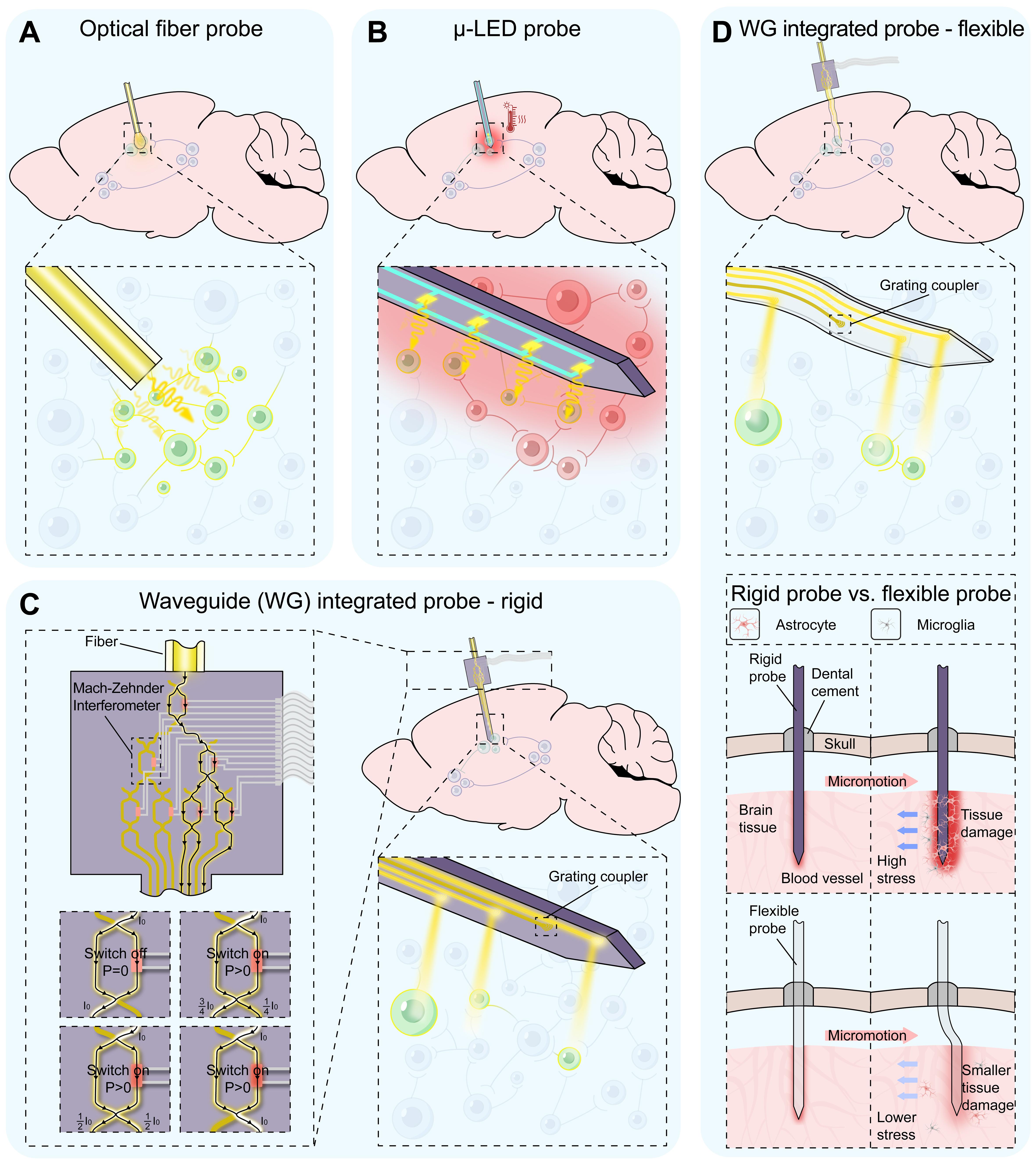
Figure 1. A schematic diagram comparing (A) fiber-optic type, (B) μ-LED type, and (C) rigid/(D) flexible waveguide integrated optogenetic probe technologies. μ-LED: Micro-light-emitting diode.
These limitations motivate a paradigm shift from source-centric illumination toward networked optical delivery in optogenetic probes. Rather than increasing the number of embedded light sources[25,26] or optical fibers, another strategy is to decouple light generation from light delivery by distributing optical power through engineered photonic networks. In this framework, optical waveguide routing architectures based on integrated photonics define how light is spatially apportioned and dynamically reconfigured across multiple stimulation sites [Figure 1C]. Importantly, the light source can be physically separated from the brain tissue, so that the primary heat-generating component is not directly implanted at the neural stimulation site. This system-level thermal-source separation reduces local thermal load in tissue and becomes particularly advantageous for dense, multi-site, and reconfigurable optogenetic stimulation.
Integrated optical waveguide routing builds upon decades of advances in integrated photonics[27], in which waveguide-based routing networks have enabled breakthroughs in optical communication[28,29], on-chip sensing[30,31], and photonic information processing[32,33]. Lithographically defined waveguides, splitters, couplers, and switching elements provide deterministic control over light propagation, scalable one-to-many distribution, and reconfigurable network topologies within compact footprints[34]. Bringing these architectures from planar chips to implantable probes introduces distinct constraints, such as tight shank real estate, limited electrical/thermal budgets, and chronic in vivo stability, underscoring the value of compact, programmable routing networks. When translated to neural interfaces, optical delivery is governed by waveguide routing topology and tunable weights rather than the physical placement of light sources, enabling high-density, multiregional, and depth-resolved stimulation while mitigating thermal and scalability constraints. While integrated optical waveguide routing has been successfully demonstrated in rigid optogenetic probes[35-37], mechanical mismatch between rigid devices and soft brain tissue can induce micromotion, inflammation, and long-term instability [Figure 1D]. In contrast, flexible probes provide mechanical compliance and geometric adaptability, enabling conformal interfacing with complex neural structures and more stable chronic implantation, while also supporting access to curved and distributed brain regions, a capability already demonstrated in flexible electronic brain-computer probes[38,39]. Extending integrated optical waveguide routing to flexible and soft platforms, therefore, represents not only a mechanical necessity but also a system-level opportunity, in which new routing architectures can be realized provided that routing fidelity is preserved under bending, stretching, and heterogeneous mechanical environments.
This review is structured to elucidate integrated optical routing as a central enabling paradigm for optogenetic probes [Figure 2]. We first introduce the fundamental principles of optical routing in integrated photonic systems, including waveguide-based light confinement, power splitting, coupling, switching, and network architectures relevant to neural interfaces. We then survey representative implementations of optical routing in rigid optogenetic probes, highlighting how routing strategies enable scalable, multiregional, and depth-resolved optical control. Finally, we examine the transition from rigid to flexible and soft platforms, focusing on how mechanical compliance and material heterogeneity reshape routing design, performance, and long-term bio-integration, and conclude with an outlook on emerging challenges and opportunities for flexible photonic-networked optogenetic neural interfaces.
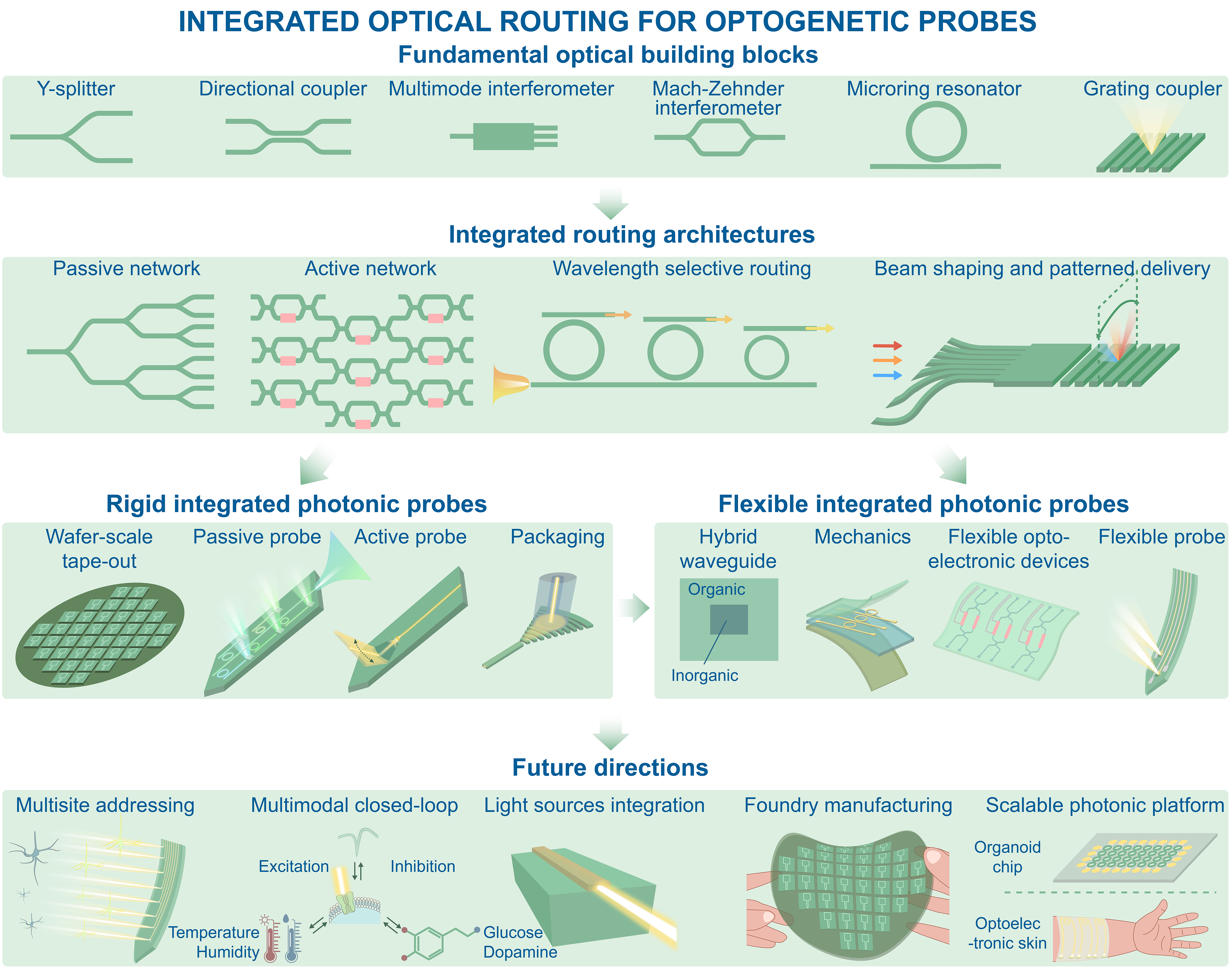
Figure 2. Organization of this review.
FUNDAMENTALS OF INTEGRATED OPTICAL ROUTING
Integrated optical routing enables controlled redistribution of light within implantable optogenetic probes. Despite the diversity of reported device geometries, including Y-branches, directional couplers, multimode interferometers, and mesh networks, the governing physics is unified. Optical routing can be understood as guided-wave mode evolution shaped by perturbations to the refractive-index landscape, which in turn control phase, coupling, and loss. This section provides a minimal mechanism-based framework for describing routing, independent of specific device implementations or platform materials.
Waveguides and modes: the physical basis of routing
Optical waveguides are the fundamental building blocks of integrated photonic systems, providing spatially nonuniform dielectric structures that confine and guide light. Common waveguide geometries include slab, rib, and strip waveguides[40] [Figure 3], all of which consist of a high-index core surrounded by lower-index cladding to achieve optical confinement and guided propagation through principles of guided-wave optics. Slab waveguides confine light in only one transverse dimension, leading to significant lateral field spreading and limited applicability for compact routing[41]. In contrast, rib and strip waveguides provide two-dimensional modal confinement and are therefore more suitable for integrated routing[42]. While rib waveguides can exhibit low loss for transverse-electric modes, their relatively weak confinement results in large bending radii. Strip waveguides offer stronger modal confinement, tighter bending radii, reduced inter-waveguide crosstalk, and favorable compatibility with fabrication, making them the most widely adopted geometry in integrated optical routing.
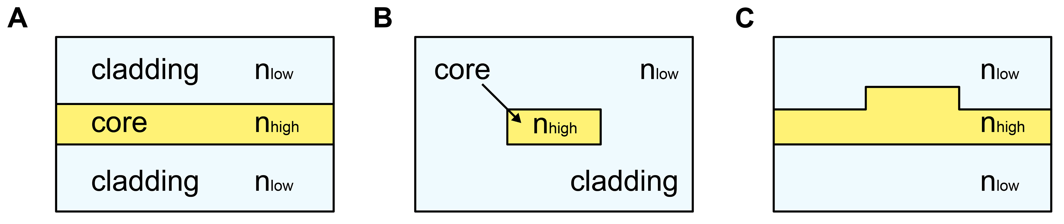
Figure 3. Schematic diagram of waveguide types: (A) slab; (B) strip; (C) rib.
Splitting and interferometers: the core routing operations
Despite the diversity of routing architectures reported to date, most integrated optical routing schemes can be broadly grouped by how optical power is redistributed, with interferometric routing representing a central class[43,44]. In integrated photonics, interferometric routing exploits the wave nature of light to steer optical signals through controlled interference. Using waveguides together with integrated splitters/combiners, such as Y-junctions[45] and Mach-Zehnder interferometers (MZIs)[46], the input field is first divided into two or more coherent branches, where the relative phase and amplitude are precisely engineered (e.g., via path-length imbalance) before recombination. The resulting constructive/destructive interference deterministically selects output ports and enables key functions, including routing, switching, and signal processing in photonic integrated circuits[47,48]. From a device-physics perspective, the splitter/combiner is not merely a passive divider but a mode-transforming element that sets the boundary conditions for subsequent interference. Common splitter implementations include Y-branches (based on adiabatic mode evolution and geometric bifurcation)[49], directional coupler-based splitters (based on evanescent coupling)[50], and multimode interference (MMI) splitters (based on self-imaging in multimode sections)[51]. These alternatives offer different trade-offs in excess loss, imbalance tolerance, bandwidth, and fabrication robustness, which directly affect phase stability and routing fidelity in interferometric networks.
Switching and modulating: from static to programmable routing
Beyond static power distribution, many optogenetic applications require dynamic and programmable control of optical routing[1,2,52]. Reconfigurability is typically achieved by actively modifying the refractive index landscape, thereby altering mode evolution, phase accumulation, or coupling strength[53-55]. In practice, this is often realized through the thermo-optic effect, where temperature-induced index changes enable phase control and thus optical path switching or redirection. Devices based on this principle are generally referred to as thermo-optic modulators or switches, and typically exhibit microsecond-scale response times[56], which are compatible with the temporal dynamics required for optogenetic neural modulation[1]. The thermally induced phase shift can be expressed as[57]:
where Δφ is the phase variation, λ0 is the operating wavelength, dn/dT is the thermo-optic coefficient (TOC) of the waveguide material, L is the heated interaction length, and ΔT is the temperature change. This relation indicates that efficient modulation favors materials with a large TOC. Representative refractive indices and TOCs of commonly used visible-wavelength waveguide materials are summarized in Table 1.
Refractive index and TOC of visible waveguide materials
| Materials | Refractive index | TOC (K-1) |
| Silicon nitride (Si3N4) | 2.02[58] | 2.0 × 10⁻⁵[59] |
| Titanium dioxide (TiO2) | 2.43[48] | -0.5 to -2.4 × 10⁻⁴[59-61] |
| Alumina (Al2O3) | 1.65[62] | 2.75 × 10⁻⁵[63] |
| Silica (SiO2) | 1.45[62] | 1.0 × 10⁻⁵[64] |
| SU-8 | 1.60[48] | -1.87 × 10⁻⁴[65] |
| Colorless polyimide (CPI) | 1.72[48] | ~-10-4[57] |
| Parylene-C | 1.639[66] | - |
| PDMS | 1.4[66] | - |
At present, the most common thermo-optic switches (TOSs) are based on micro-ring resonators (MRRs) and MZIs. As shown in Figure 4, in MRR based TOSs, light is launched into a straight bus waveguide and subsequently coupled into a neighboring ring waveguide through evanescent-field interaction. The optical field circulates within the ring and, at each round trip, partially couples back to the bus at the coupling region. When the input wavelength satisfies the resonance condition, the optical signal is transferred to the drop port; otherwise, it remains at the through port. The resonance condition requires that the round-trip phase accumulation in the ring equals an integer multiple of 2π, which can be expressed as: βL = 2πm, where β is the propagation constant in the ring, L is the ring circumference, and m is the resonance order. The corresponding wavelengths are referred to as resonant wavelengths, and the spacing between adjacent resonances defines the free spectral range (FSR). Because the effective refractive index (neff) of the ring waveguide can be conveniently tuned via physical mechanisms such as the thermo-optic effect, the resonance condition can be dynamically shifted. This enables controlled switching between the drop and through ports, allowing MRRs to serve as compact and efficient TOSs.

Figure 4. Schematic diagram of the working principle of the MRR type TOSs. MRR based switching element with two parallel waveguides at the (A) OFF and (B) ON states, and with two cross waveguides at the (C) OFF and (D) ON states. The black arrow indicates the direction of light propagation in the waveguide-coupled resonator. MRR: Micro-ring resonator; TOSs: thermo-optic switches.
The MZI structures are widely used in integrated photonics for modulators, optical switches, and filters. Compared with resonant devices such as MRRs and Bragg gratings, MZI-based architectures generally offer broader operating bandwidth and greater fabrication tolerance. A typical MZI TOS consists of two 3-dB couplers and two phase-shift arms. The 3-dB couplers can be implemented using Y-branches, directional couplers, or MMI couplers. Among these, MMI-based MZI switches are particularly attractive due to their simple fabrication, compact footprint, large process tolerance, and low cost. They can be readily cascaded into large-scale switching matrices, exhibit microsecond-level switching speeds, provide wide optical bandwidth, and show low polarization sensitivity, making them well-suited for scalable routing networks[67-69]. As shown in Figure 5, in a typical 2 × 2 MMI-MZI switch, light entering port 1 or port 2 is evenly split by the first 2 × 2 MMI coupler into two beams with equal amplitude and phase, which propagate through the two interferometer arms. Localized heating modifies the temperature in one phase-shift arm, thereby changing the local refractive index and introducing a controllable phase difference between the two paths. After recombination in the second 2 × 2 MMI coupler, interference directs the output to port 3 or port 4. Consequently, optical path switching between the two output ports can be achieved by tuning a single-phase shift arm. TOSs based on the two architectures described above have begun to be adopted in optogenetic probes and will be discussed in detail in Section “Rigid Integrated Photonic Platforms for Optical Routing in Optogenetics”.
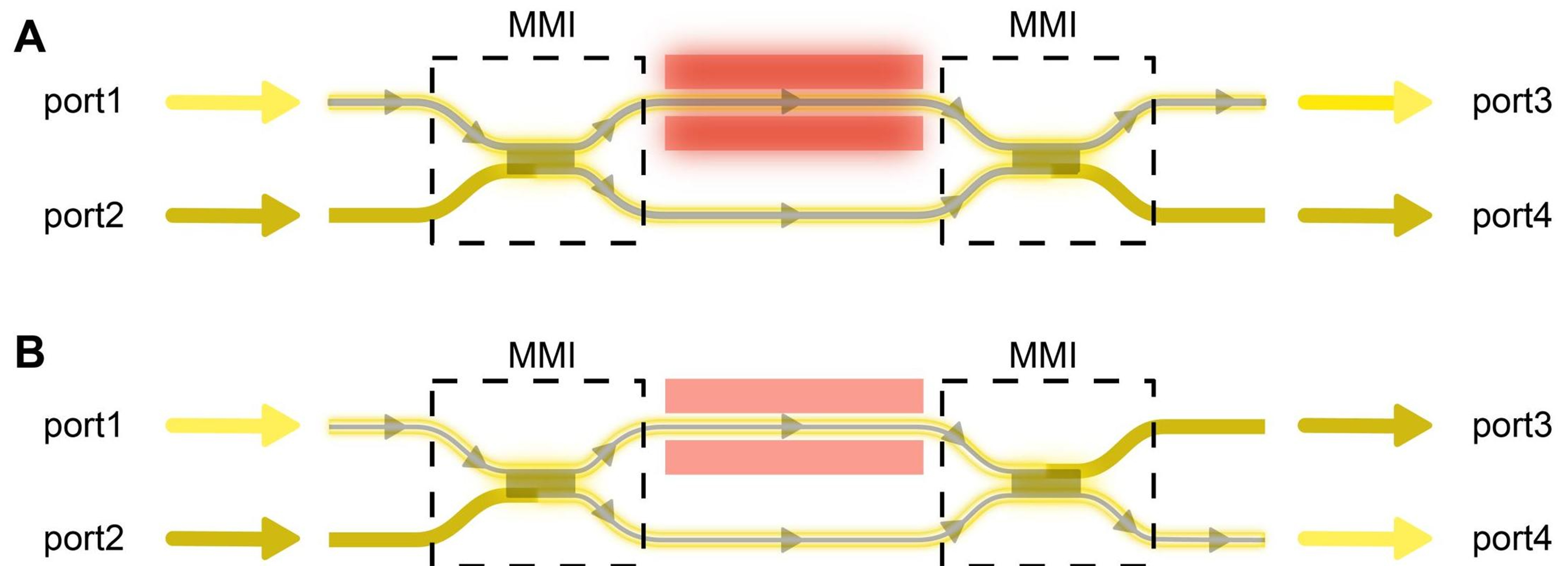
Figure 5. Schematic diagram of the working principle of the MMI-MZI type TOSs: (A) “bar” status; (B) “cross” status. The arrow indicates the direction of light propagation in the yellow-highlighted waveguide. Deep red sections represent the heating electrodes with voltage applied, while light red ones indicate electrodes with no applied voltage. MMI: Multimode interference; MZI: Mach-Zehnder interferometer; TOSs: thermo-optic switches.
Grating couplers: from guided waves to tissue illumination
In waveguide-routing-enabled optogenetic probes, light carried by the on-probe waveguide network must ultimately be emitted into the targeted neural cells or tissue. Grating emitters serve as passive optical out-couplers and do not generate local Joule heat at the emission site, aside from tissue absorption of the delivered light. This passive-emitter architecture differs from direct-emitting μ-LED-based approaches, in which electrical power is dissipated locally at or near the stimulation site. Moreover, because scattering in neural tissue is highly anisotropic, grating emitters and optical phased arrays can be engineered to exploit directional transport for beam forming and shaping[36,70,71]. Accordingly, grating couplers constitute the canonical out-of-plane interface in routing-enabled optogenetic probes. Grating couplers[72] convert on-chip guided modes into free-space beams via a longitudinally periodic refractive-index modulation that supplies the grating momentum for Bragg-type phase matching to radiated diffraction orders. Under phase matching, a controlled fraction of power is diffracted out of plane at a designed emission angle. The emission angle, divergence, and polarization selectivity are mainly governed by the grating period, duty cycle, and etch depth through their effects on the effective index and grating wavevector. With footprints typically on the order of ~20 × 20 μm2, grating couplers are compatible with high-spatial-resolution stimulation that approaches near-single-cell targeting.
Constraints unique to optogenetics: from integrated photonic design to in vivo requirements
Because the waveguide routing section of an integrated photonic probe must be implanted into brain tissue and operate chronically in a complex in vivo milieu, deep-brain optogenetic applications impose a set of nonstandard design and fabrication constraints that clearly distinguish neural photonic probes from conventional on-chip photonic integrated circuits. First, strong visible-light scattering in brain tissue, together with regional variations in composition, density, and refractive index, imposes stringent requirements on emission angle, beam divergence, and the effective output-power threshold. Precise control of directionality and divergence is essential to deliver sufficient stimulus while minimizing unintended activation of nearby neurons[73]. Second, high-density output sites demand high spatial selectivity; optical leakage or unintended coupling between channels directly degrades specificity, particularly in dense waveguide networks, necessitating sufficiently low inter-channel crosstalk and a large extinction ratio
RIGID INTEGRATED PHOTONIC PLATFORMS FOR OPTICAL ROUTING IN OPTOGENETICS
Rigid integrated photonic platforms are implemented as waveguide networks on implantable silicon shanks (“neurophotonic probes”), providing a microfabrication-compatible[46] and experimentally validated approach for deep-brain, multi-emitter optogenetic stimulation[74]. Such waveguide networks can be implemented on slender probe shanks to access deep brain regions, since high-index-contrast (HIC) waveguide material systems and mature micro/nanofabrication processes[75] enable compact photonic components with small bend radii, small footprints, and tight dimensional control, well-suited for dense integration of on-probe emission sites[35,70,76,77]. Over the past decade, diverse rigid probe architectures have demonstrated integrated waveguide routing networks, reconfigurable switching matrices, and on-chip or heterogeneously integrated light sources, advancing waveguide routing from a concept to functional neural-interface systems. This section reviews rigid-platform implementations from five perspectives: materials and waveguide technologies, on-shank network architectures, reconfigurable routing strategies, active emitter integration and packaging, and limitations in optogenetic applications.
Rigid material platforms and waveguide technologies
Because optogenetics operates in the visible, the choice of low-loss, transparent waveguide materials and platform technology directly sets the attainable integration density, propagation loss, and footprint of integrated photonic probes. HIC and visible-transparent waveguide materials, such as SiN[78-80], Al2O3[81] and TiO2[82-84], enable strong modal confinement, small bend radii, and compact routing building blocks, which are essential for on-shank networks constrained by limited shank width and cross-sectional area. As channel counts scale, propagation loss becomes the dominant system bottleneck; in the visible, fabrication-induced sidewall scattering is typically more limiting than in telecom photonics[85]. Recent advances in foundry and lab-level process optimization and materials engineering have substantially improved the feasibility of low-loss rigid visible-light routing platforms [Table 2], which are increasingly being adopted for optogenetic probes. Among these options, SiN remains the dominant material system for rigid optogenetic probes due to its CMOS compatibility, scalability to volume manufacturing, and favorable biocompatibility.
Summary of visible light waveguide material platform technologies and their applications in optogenetics
| Materials | Process platform | Propagation loss (dB/cm) (wavelength, nm) | Institution | Year | Applications in optogenetics: (dimensions, wavelength, and feature parameters) |
| SiN | 8-inch foundry | 1.02 (443) 0.3 (532) 0.11 (635) | Interuniversity Microelectronics Center (IMEC) | 2024[86] | Neuropixels Opto probes[37]: MZI-MMI array, dual-color emitters [(16 × 25 μm2, 450 nm, 638 nm), 14 sites per color] |
| SiN | 8-inch foundry | 1.0-4.6 (466-500) 0.8-2.7 (502-550) 0.6-1.9 (552-600) 0.5-1.4 (602-648) | Advanced Micro Foundry (AMF) | 2019[46] | Nanophotonic probes[70]: emitter (6 × 24.6 μm, 488 nm); Beam steering probe[71]: optical phased array (0.006-0.011 mm2, 460-598 nm, steering Arc length: 33.0-113.0 μm, 4 channels) |
| SiN | 6-inch foundry | 1 (518-541) | Qaleido Photonics | 2025[87] | No optogenetic probe validation reported |
| SiN | 8-inch foundry | 2.5-0.8 (532-673) | SITRI | 2024[88] | No optogenetic probe validation reported |
| SiN | Lab | 1.2 (488) 0.2 (532) 0.06 (644) | Columbia University | 2024[85] | Reconfigurable nanophotonic probes[35]: MZI-MMI TOS (473 nm, ON/OFF contrast 17 dB, power: 30 mW); 8 emitters (20 × 20 μm2, 473 nm) |
| Al2O3 | 8-inch foundry | 0.18 (450) 0.03 (532) | IMEC | 2025[89] | No optogenetic probe validation reported |
| Al2O3 Al2O3 | Lab Lab | 0.36 (405) 1.39 (637) | SINTEF Fujitsu Research | 2025[90] 2025[91] | No optogenetic probe validation reported No optogenetic probe validation reported |
| TiO2 TiO2 | Lab Lab | 5.46 (589) 7.8 (633) | Westlake University University of Twente | 2025[48] 2020[83] | No optogenetic probe validation reported No optogenetic probe validation reported |
Passive waveguide routing networks on rigid shanks
In rigid optogenetic probes, integrated optical routing networks are typically embedded directly along the probe shank [Figure 6A], distributing light from one or a few inputs to multiple spatially separated emission sites, enabling depth-resolved, high-spatial-resolution, region-selective excitation or inhibition. Early multi-site designs largely relied on cascaded splitters such as Y-branches[45] and directional couplers[92], with output ports positioned at different locations along the shank; however, increasing the channel count in such splitter-based schemes generally requires large-area arrays. To reduce footprint, Lanzio et al. exploited wavelength-division multiplexing by coupling a single waveguide to five MRRs (radius < 4 μm) as passive nanophotonic switches[93] [Figure 6B-D], alleviating spatial constraints in nanophotonic links. Through 3D integration of a compact sensor array with the nanophotonic link, this scalable architecture can increase sensor density per cross-section by an order of magnitude relative to state-of-the-art devices. Nevertheless, MRRs operate at specific resonance wavelengths and require stringent environmental control to stabilize the spectrum and maintain consistent switching performance, imposing tighter demands on fabrication and system-level stability.
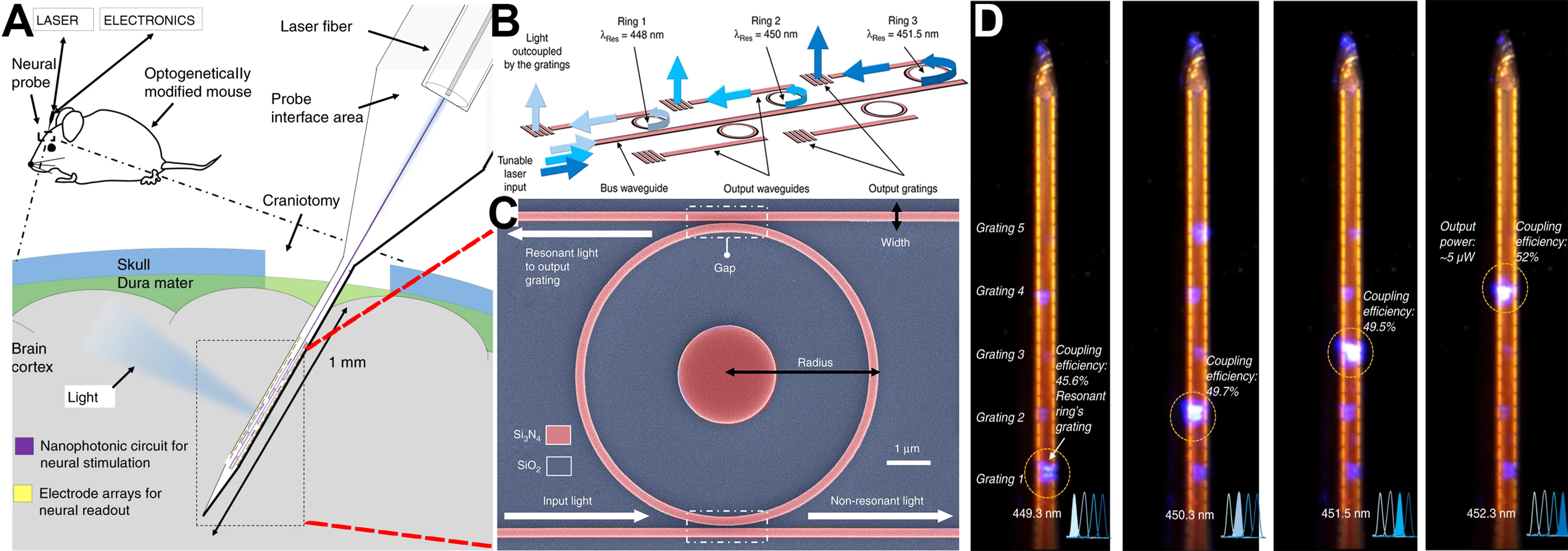
Figure 6. Small footprint and passive optoelectrode for electrophysiology and optogenetic applications[93]: (A) Schematic illustration of the neural probe; (B) Schematic illustration of the nanophotonic circuit in the probe tip area; (C) SEM image of a SiN ring resonator; (D) Optical microscope image of the tip of the assembled neural probe. This figure is adapted from Ref.[93]. Copyright © 2021 The Author(s). SEM: Scanning electron microscopy.
Despite these advances, most routing networks on rigid probes remain passive: optical power distribution is fully determined by fixed splitting ratios and static routing defined at the design stage. Consequently, channels are often turned on and off collectively, and individual emission sites cannot be independently or dynamically controlled once the device is fabricated; the output pattern is likewise constrained to a predetermined spatial distribution. This lack of per-channel addressability limits experimental flexibility, particularly for adaptive targeting across multiple brain regions or neuronal populations. These constraints motivate the introduction of reconfigurable integrated photonic elements and switching matrices to enable dynamic channel selection and programmable power distribution, as discussed in the next section.
Reconfigurable routing on rigid waveguide integrated probe
To overcome the fixed power distribution and limited channel addressability of passive waveguide networks, rigid integrated photonic probes have increasingly incorporated reconfigurable waveguide devices that enable dynamic path selection and power reallocation. Building on the phase-control and coupling-modulation mechanisms discussed in Section “Fundamentals of Integrated Optical Routing”, reconfigurable networks extend rigid probe platforms from static splitter trees to programmable photonic routing systems, and further support advanced architectures that combine spatial routing with wavelength-division and channel-multiplexing strategies. Mohanty et al. implemented a SiN reconfigurable TOS array based on MMI-MZI switches to realize eight independently controllable emitters (The divergence angle of the emitted light beam is 2.2° transverse to/3.75° along the waveguide propagation)[35], and integrated electrophysiological electrodes to achieve single-neuron-resolution optogenetic stimulation and recording in the hippocampus. Lakunina et al. further combined an MMI-MZI TOS architecture with Neuropixels[37], integrating two sets of 28 optical stimulation sites alongside 960 recording electrodes (14 sites for stimulation and 14 sites for inhibition) [Figure 7A and B], thereby enabling in vivo high-quality excitation and inhibition recordings [Figure 7C] with spatially addressable optogenetic modulation across cortical depths.
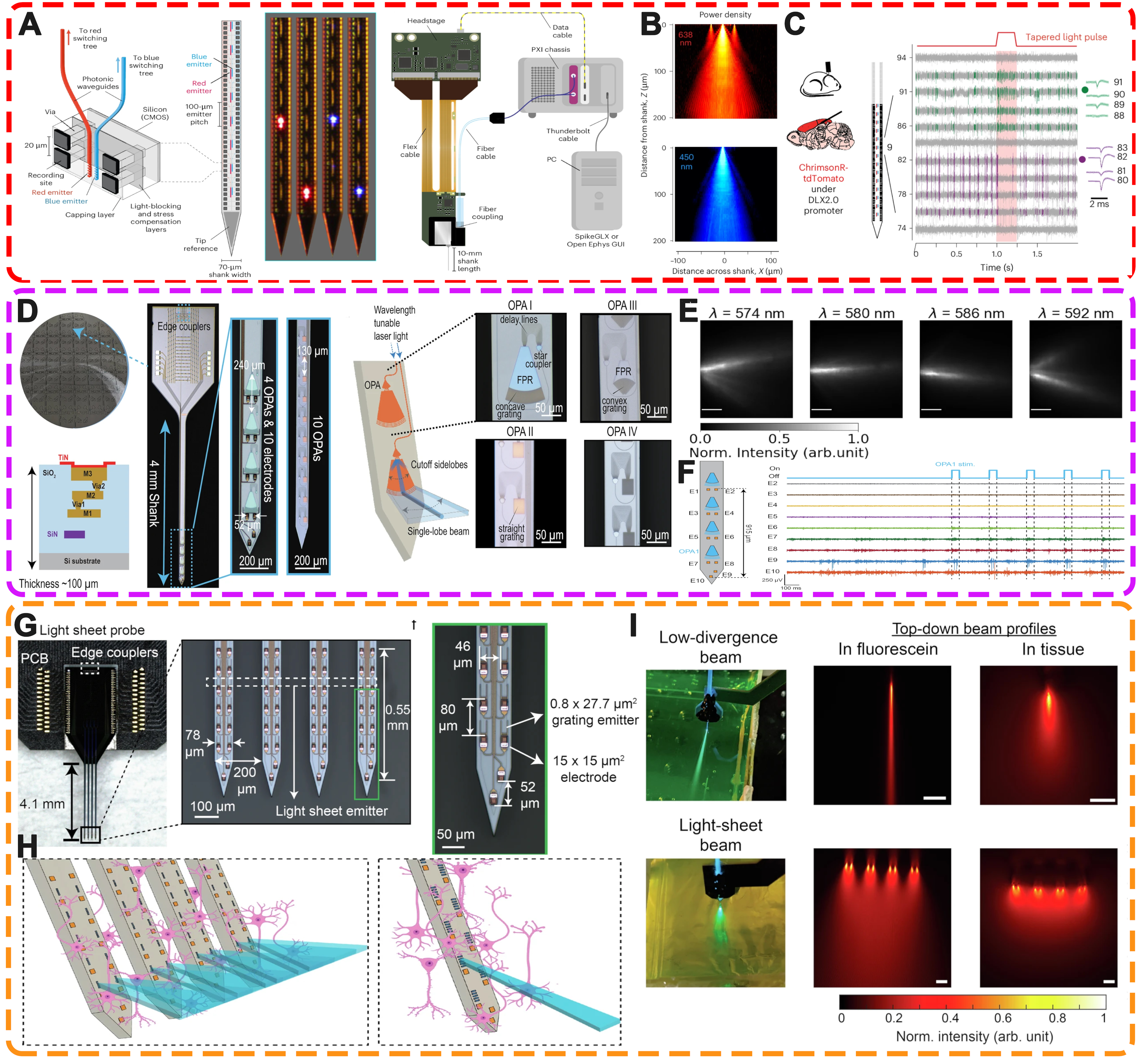
Figure 7. Neuropixels Opto[37]: (A) Design of the prototype Neuropixels Opto probe; (B) Top view of light propagation from a red and blue emitter; (C) Neuropixels Opto to drive localized network effects. (A-C) are reprinted with permission from Ref.[37], Copyright © 2026 The Author(s). Nanophotonic phased arrays probe[71]: (D) Foundry-fabricated neural probes with single-lobe beam-steering OPA; (E) Measured top-down intensity beam profiles in fixed tissue; (F) Demonstration of optogenetic stimulation and electrophysiological recording. (D-F) are reprinted with permission from Ref.[71], Copyright © 2024 The Author(s). Light-sheet probes[70]: (G) Optical micrographs of probes; (H) Conceptual illustration of the nanophotonic neural probe system; (I) Top-down view of the low-divergence beam and the light sheet beam propagating. (G-I) are reprinted with permission from Ref.[70], Copyright © 2025 The Author(s). OPA: Optical phased-array; CMOS: complementary metal–oxide–semiconductor; PXI: PCI eXtensions for instrumentation; PC: personal computer; PCB: printed circuit board.
However, owing to the relatively small TOC of SiN, the power consumption of a single TOS can reach
Taken together, these rigid photonic probes represent complementary routes toward reconfigurable and structured optogenetic stimulation. Reconfigurable nanophotonic probes based on MMI-MZI TOS arrays, such as Neuropixels Opto[37], emphasize depth-resolved, localized, and electrode-compatible optical addressing by integrating dual-color stimulation sites with high-density electrophysiological recording electrodes. However, their addressability is restricted to predesigned emitter locations, and their scalability is limited by TOS power, routing complexity, and system interconnects. OPA probes shift the emphasis from discrete site selection to programmable beam steering, enabling selectable stimulation within a defined scanning range (a single OPA scanning arc length of up to 235 μm[71]) while avoiding high TOS array power through delay-line- based passive phase control. Nevertheless, they require precise phase design or wavelength-swept laser control, and their current scanning range still cannot cover the entire implanted probe region. Light-sheet probes[70] further extend rigid waveguide routing from point-like emission to engineered illumination profiles, enabling low-divergence or sheet-like excitation over defined tissue volumes and expanding the functionality toward imaging. However, their addressability is mainly determined by predefined emission ports along the shank and is therefore depth-resolved rather than continuously scanned, as in OPA probes. Importantly, these three strategies have all demonstrated in vivo optical modulation with simultaneous local electrophysiological recording, indicating that rigid integrated photonic probes can support increasingly powerful combinations of addressable stimulation, beam-profile engineering, and electrode-compatible neural readout. Future rigid photonic probes are expected to evolve toward integrated architectures that overcome current limits in switching power, beam-steering range, routing density, and optoelectronic co-design, enabling more scalable and programmable high spatiotemporal-resolution optogenetic interrogation.
Active emitters integrated and heat management technologies
Beyond routing waveguides and switching networks, the overall performance and scalability of integrated photonic probes depend strongly on system-level implementations of light sources, packaging, and interconnects. At present, optical packaging for integrated photonics still relies predominantly on butt-coupling to optical fibers, which can introduce practical cable-management issues in long-term biological experiments. To address this, as shown in Figure 8, Kampasi et al. coupled dual-wavelength injection laser diodes into monolithically integrated on-shank SiON waveguides using gradient-index (GRIN) relay optics, enabling multisite, dual-color light delivery alongside dense recording electrodes, and the laser diodes were wirelessly controlled[97]. Importantly, temperature rise induced by source dissipation must be carefully managed. GRIN optics provide high coupling efficiency, allowing lower diode output power and thus reduced heat generation, an advantage for scaling to more channels. Moreover, GRIN elements act as effective thermal insulators[98], physically separating the heat source from the probe shank and suppressing heat conduction toward brain tissue. Thermal simulations and measurements indicate that combining GRIN-enabled thermal isolation with high-efficiency optical coupling is a key engineering route to scale high-density optogenetic integrated probes without excessive tissue heating.
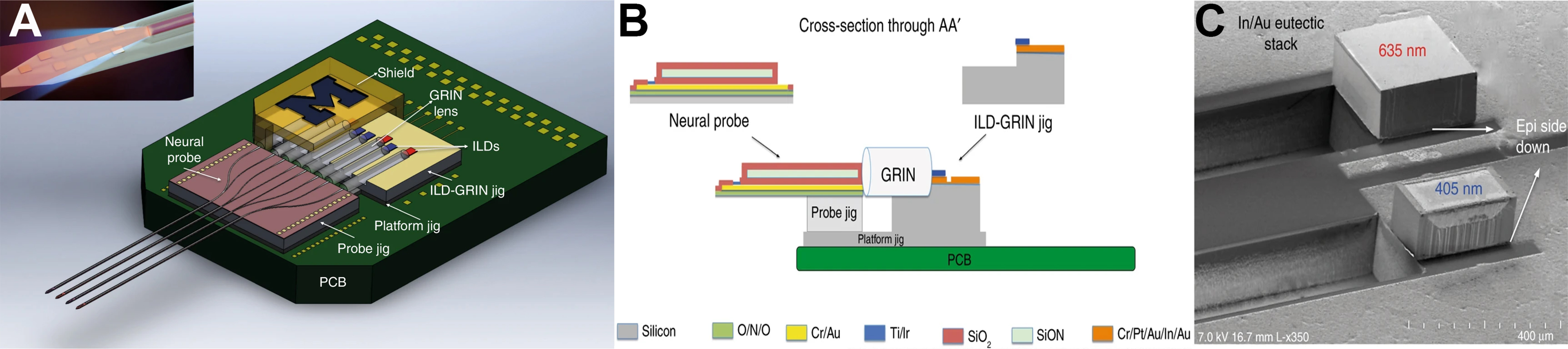
Figure 8. Schematic of multishank multicolor fiberless optoelectrode assembled on a printed circuit board[97]: (A) Device fabrication details; the inset is the local enlargement of the tip of the probe; (B) Fabricated neural probe shank tips with monolithically integrated dielectric waveguides; (C) High-magnification SEM image of epi-side down flip-chipped 405 and 635 nm ILDs on the ILD-GRIN. This figure is adapted from Ref.[97]. Copyright © 2018 The Author(s). SEM: Scanning electron microscopy; ILDs: injection laser diodes; GRIN: gradient-index; PCB: printed circuit board.
In addition to source heating, heat generated by tuning elements also warrants attention. Mohanty et al. estimated the thermal impact of MMI-MZI-based thermo-optic switching networks, reporting a probe-tip temperature rise of ~0.2-0.4 °C, which can be regarded as an upper bound for the surrounding tissue and remains well below safe operating limits (< 2 °C)[35]. Because the micro-heaters are located outside the brain, thermo-optic heating is spatially separated from the target tissue. Further incorporating heat sinks and optimizing heater design[99] could suppress heat conduction toward the implanted probe region and support higher emitter counts. This also highlights a practical advantage of waveguide-integrated approaches over
Limitations of rigid waveguide routing for optogenetics
From a photonics and manufacturing perspective, rigid waveguide integrated optogenetic probes, particularly those based on SiN and related dielectric platforms have demonstrated strong performance advantages. The SiN platform is highly compatible with scalable wafer-level fabrication and benefits from mature process design kits (PDKs), well-characterized material stacks, and reproducible patterning workflows. As a result, rigid integrated waveguide devices can offer high geometric precision, stable optical confinement, predictable splitter/coupler behavior, and good long-term parameter stability[88,100]. HIC further enables small bend radii and dense on-shank routing layouts, allowing compact routing elements and multisite light delivery with controlled loss and crosstalk. Collectively, these attributes make rigid platforms well-suited for complex routing networks, switching matrices, and multiplexed optical distribution architectures.
However, in chronic implantation and behaviorally relevant settings, these advantages come with inherent limitations. Rigid probes exhibit pronounced mechanical mismatch with soft brain tissue[101]. During long-term implantation, the brain undergoes continuous microscale motion driven by pulsation, respiration, and head movement, which is further amplified in freely moving experiments. Because rigid shanks cannot accommodate such deformation, persistent probe-tissue micromotion can elicit inflammatory responses, degrade electrophysiological recording stability, and gradually alter the local optical emission geometry. For routing-based optogenetic probes, this mechanical mismatch can also disrupt the spatial registration between emission sites and targeted neural populations, reducing the repeatability of stimulation over time. Together, these considerations indicate that while rigid routing platforms provide a necessary foundation for high-density, precisely defined optical routing, their mechanical and bio-interface constraints impose intrinsic limits on long-term stability and large-scale in vivo deployment, motivating a transition toward mechanically compliant flexible routing platforms[38].
TRANSITION FROM RIGID TO FLEXIBLE: OPTICAL ROUTING UNDER MECHANICAL CONSTRAINTS IN OPTOGENETICS
Flexible integrated waveguide platforms can be viewed as a natural extension of rigid photonic probe technologies: they inherit the core concepts of rigid waveguide routing, yet must function under fundamentally different mechanical constraints. Although many rigid platform device architectures can, in principle, be ported to compliant substrates, mechanical compliance introduces deformation-driven effects that directly perturb optical performance and long-term stability. Bending, strain, and multilayer deformation alter the waveguide effective index, phase accumulation, and coupling coefficients; without deformation-aware design, these perturbations can cause mode mismatch, increased loss, and even device failure. Consequently, flexible waveguide platforms require coordinated co-design across mechanics, materials, and photonic structures rather than a simple process transfer. This section reviews the rigid-to-flexible transition from three perspectives: flexible materials and waveguide platforms, mechanical design principles under deformation, and the evolution of integration pathways and the functionalities they unlock, with current flexible waveguide optogenetic probes as a focal point to briefly discuss development trends and key engineering bottlenecks for scalable manufacturing and validation.
Flexible materials and waveguide platforms
For flexible waveguide-based optogenetic probes, the overall probe stiffness is jointly determined by geometry and the Young’s modulus of the constituent materials[102]. Accordingly, chronic tissue responses after implantation are coupled not only to intrinsic material properties but also to probe form factor. Implantable neural probes are typically designed as slender, high-aspect-ratio structures to minimize cross-sectional area and thereby reduce tissue damage during insertion. Mechanically, such structures can be approximated as cantilever beams, whose bending stiffness is determined by both the material modulus[7] and the cross-sectional geometry[103]. For a rectangular probe shank, the bending stiffness is expressed as: k = Et3b/4L3, where E, t, b and L are the Young’s modulus, thickness, width and length of the implanted probe segment, respectively. For a cylindrical probe, k = 3πEd4/64L3, where E, d and L are the Young’s modulus, diameter and length of the implanted probe segment, respectively. Thus, bending stiffness depends not only on the material modulus but also strongly on the probe geometry, scaling cubically with thickness for rectangular probes and quartically with diameter for cylindrical probes. Therefore, selecting low-Young’s-modulus materials and reducing probe dimensions are both important strategies to improve mechanical compliance and mitigate long-term inflammatory responses driven by post-implantation micromotion. Table 3 summarizes the Young’s moduli of commonly used waveguide materials. Compared with conventional inorganic photonic waveguide materials, polymers generally exhibit much lower moduli, thereby reducing the effective probe stiffness when combined with appropriate probe geometries. In addition, the ease of processing and low-loss characteristics of polymer waveguides further make them attractive for flexible probe fabrication.
Mechanical properties of biomaterials
However, from an integrated waveguide routing perspective, polymer waveguides typically offer only a low refractive-index contrast between the core and the cladding/substrate, thereby limiting optical confinement. Suppressing bend radiation loss, therefore, often requires larger lateral dimensions and larger bend radii[111], which work against high-density integration. This constraint becomes particularly acute when attempting to realize high channel counts, multi-stage power splitting, and many emission sites within a shank of limited width (e.g., < 100 μm). Motivated by these limitations, recent studies have explored incorporating higher index, low absorption inorganic material systems on flexible substrates, such as silicon-based materials[112], inorganic oxides[113], and chalcogenide glasses (ChGs)[114], to achieve stronger modal confinement and more compact functional photonic structures on compliant platforms[115,116]. Furthermore, hybrid organic/inorganic integration schemes with an “inorganic core and polymer cladding” are considered intrinsically advantageous for compact flexible photonic integrated devices[117]: the inorganic core provides high index contrast and low-loss guiding, whereas the polymer cladding and substrate confer mechanical compliance and packaging compatibility. In principle, such hybrid platforms can substantially shrink routing device dimensions, enabling more stimulation sites and more complex routing topologies within small shank footprints, and thereby offering greater integration potential for near-single-cell-resolution, multi-region addressable optogenetic probes. Consequently, the choice of flexible materials and waveguide platforms first defines the attainable bounds of confinement, loss, and device size, and thus sets the integration ceiling for flexible routing within probe-scale geometries. Yet high confinement alone does not guarantee usable routing on a flexible shank: once implanted, bending and micromotion continuously perturb the effective index and coupling gaps, making deformation-robust routing a central requirement. This issue is examined in detail in the next section, “Mechanics of optical routing design”.
Mechanics of optical routing design
Material selection sets the upper bound of achievable optical confinement on flexible platforms, but it must be emphasized that flexible waveguide probes inevitably operate under bending, tensile/compressive strain, and coordinated deformation of multilayer stacks. Such mechanical perturbations modify the effective index of the routing waveguide, the optical path length, and the coupling gaps, thereby affecting phase accumulation and power distribution and imposing additional constraints on transmission spectra, device uniformity, and long-term stability.
In flexible electronics, a central paradigm for mechanical robustness is neutral plane engineering, in which functional layers are placed near the strain-neutral plane to minimize deformation-induced strain[118,119]. However, the design objectives of flexible photonic systems are more complex: fully embedding photonic components within thick claddings can improve strain isolation, but it also degrades heat dissipation and suppresses evanescent-field interactions with the surrounding medium. This interaction is essential for photonic sensing and evanescent coupling. For neural probes, integrated photonics is attractive not only for delivering stable optical stimulation but also for monitoring the brain micro-environment (e.g., temperature, humidity, and chemical changes), offering substantial promise and potential value. Device architectures, therefore, often require a trade-off between strain suppression and environmental interaction. In practice, many flexible photonic devices place functional layers near the polymer surface to enhance external coupling; however, this increases bending-induced strain and typically limits flexibility to millimeter-scale bend radii (often ≥ 5 mm[112,120,121]), thereby reducing the available deformation freedom for deployment.
To address this challenge, Li et al. proposed and experimentally validated a local multiple-neutral-axis mechanical design paradigm[117] [Figure 9A and B]. Rather than forcing all device layers onto a single neutral plane, this approach uses multilayer lamination to create multiple low-strain regions across the thickness, enabling functional partitioning: strain-sensitive, routing-critical photonic layers are placed in interior, near-central low-strain zones to suppress strain-optical coupling, while near-surface regions are preserved for evanescent field interaction or sensing interfaces. Practically, the paradigm introduces a low-shear-modulus soft interlayer [e.g., silicone/polydimethylsiloxane (PDMS)] between polyimide and SU-8. Under bending, this soft layer undergoes significant interfacial shear, reshaping strain transfer across the stack so that individual functional layers develop their own neutral planes. The positions of these neutral axes can be tuned via layer thickness and modulus, thereby tailoring the local strain distribution under bending. Figure 9C shows that tuning the cladding thickness modulates the stress experienced by the micro-disk resonator, and the resulting mathematical relationship between resonance-wavelength shift and chip bending curvature agrees with the theoretical prediction of the multiple-neutral-axis analysis. In this way, mechanics-aware design converts flexible deformation from a “random perturbation” into a designed boundary condition, providing a structural basis for maintaining stable performance of complex routed waveguide networks under deformation.
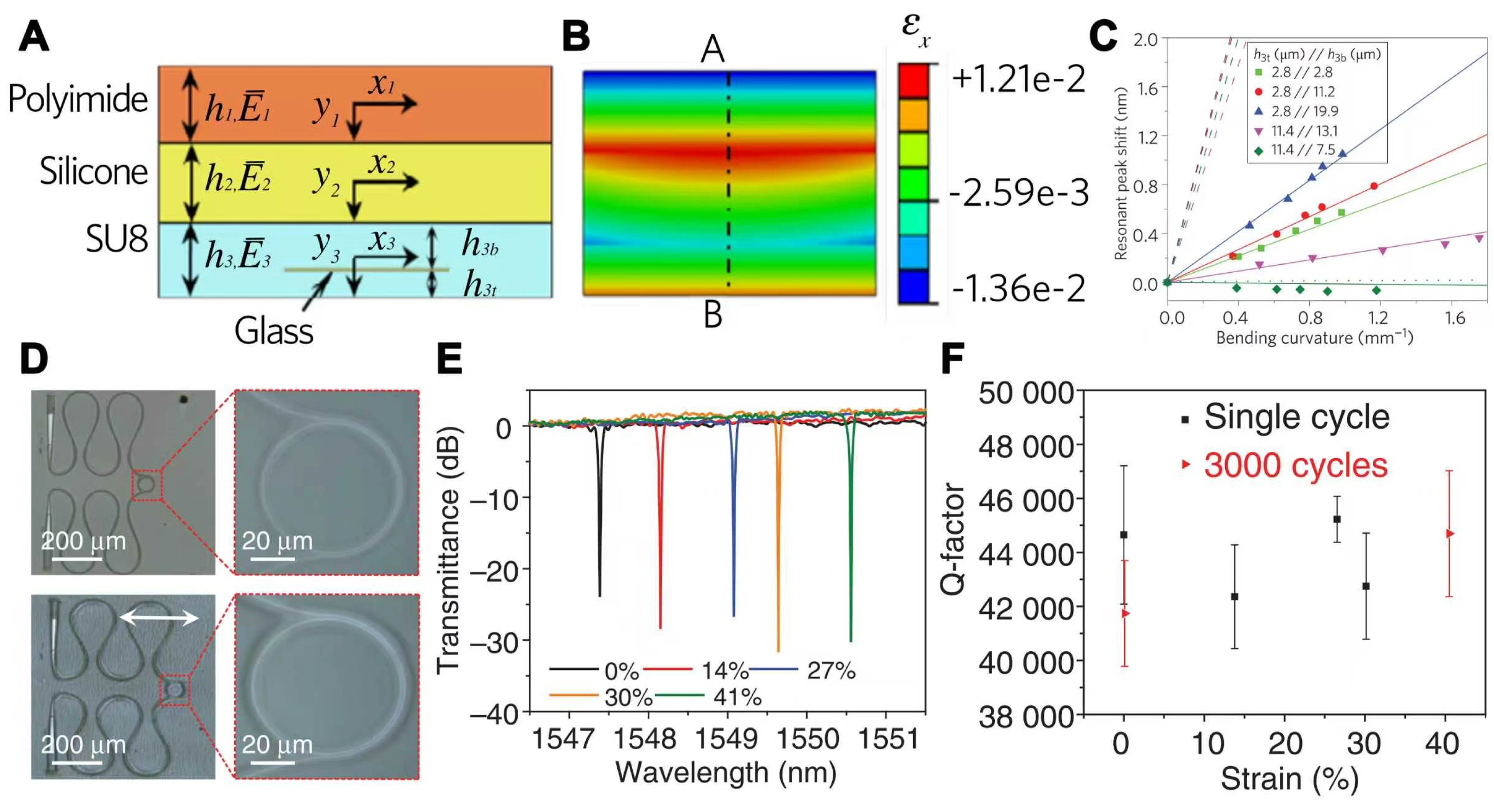
Figure 9. Multi-neutral-axis theory[117]: (A) Cross-sectional schematic of the flexible photonic chip with a PI-silicone-SU8 three-layer structure; (B) Contour plot of bending strain distribution obtained from FEM when the structure is bent; (C) Resonance wavelength shift plotted as a function of bending curvature; Symbols are experimentally measured data, solid lines are predictions made using multi-neutral-axis theory. (A-C) are reprinted with permission from Ref.[117], Copyright © 2014 Springer Nature. Integrated stretchable photonics[75]: (D) Top-view micrographs of a stretchable device; (E) normalized optical transmittance spectra of a ChG/SU-8 stretchable resonator at different nominal strain levels; (F) Q-factors of ChG/SU-8 resonator devices before and after 3,000 stretching cycles at 41% nominal strain. (D-F) are reprinted with permission from Ref.[75], Copyright © 2017 The Author(s). PI: Polyimide; FEM: finite element method; ChG: chalcogenide glass.
Beyond bending, flexible devices may also experience tensile deformation. Inspired by stretchable electronics, stretchable photonic systems commonly use serpentine/meander interconnects to transform global stretching into local bending, thereby minimizing strain in critical photonic components. Li et al. reported the first stretchable photonic devices[75]: to render intrinsically brittle inorganic-glass photonics stretchable, they employed local substrate stiffening via SU-8 encapsulation of ChG to suppress deformation of key photonic elements [Figure 9D]. At an overall elongation of 41%, the maximum strain in the Euler-spiral geometry was only 3%, demonstrating a 14× reduction and highlighting the amplification effect of geometric strain engineering [Figure 9E]. As the tensile load increases, the resonance peaks red-shift, reflecting stress-optical coupling. The interconnecting waveguides were further implemented as serpentine Euler spirals to mitigate bending-radiation loss under stretching. The platform withstood 3,000 cycles at 41% nominal strain without measurable degradation in optical performance [Figure 9F].
Existing flexible phase-sensitive photonic devices like MRR and MZI mainly report deformation-induced wavelength shifts, Q-factor changes, transmission stability, and bending/fatigue durability[105], whereas quantitative correlations between mechanical strain and extinction ratio or crosstalk remain limited because these metrics are jointly affected by coupled changes in effective index, optical path length, coupling gap, loss balance, and fabrication tolerances[75,105,117]. It is therefore expected that future studies will establish quantitative characterization methods to clarify the strain-dependent evolution of extinction ratio and crosstalk in flexible phase-sensitive photonic devices.
Overall, the mechanical design objectives of flexible photonic waveguides can be distilled into two requirements: maintaining (i) predictability of optical signals and coupling relationships under deformation; and (ii) long-term reliability of multilayer interfaces. These mechanics-aware designs define the requirements for optical routing, but probe-level scalability ultimately depends on whether manufacturing and integration can reproducibly realize the required layer stacks, stress states, and interfaces with wafer-scale uniformity across multi-channel networks, which is the focus of the next section, “Integration strategies of flexible photonic device fabrication”.
Integration strategies of flexible photonic device fabrication
In flexible integrated photonics, routing performance is ultimately realized through process execution rather than design intent alone. Deposition temperature, residual stress, etch/plasma damage, release/transfer steps, and multilayer bonding quality directly determine whether low-loss waveguides, stable couplers, and repeatable emitters can be fabricated and assembled into probe-scale networks. Building on the material bounds established in Section “Flexible material and waveguide platforms” and the deformation-aware design principles developed in Section “Mechanics of optical routing design”, this section turns to the manufacturing and integration pathways for flexible photonics and the associated photonic integrated applications.
Transfer-based integration strategy and applications
In the early development of HIC flexible waveguide integrated devices, Si and SiN-based HIC flexible waveguides were first demonstrated primarily via transfer printing approaches[122-124]. However, such hybrid integration typically requires multiple pattern-transfer steps across different substrates, imposing clear limitations on throughput, yield, and achievable integration complexity.
To address these constraints, Chen et al. introduced GeO2 as a sacrificial layer for fabricating HIC flexible photonic integrated waveguides[113] [Figure 10A]. Leveraging GeO2’s intrinsic tolerance to high-temperature and high-power plasma processes, high-quality inorganic optical films can be directly grown on its surface using a range of thin film deposition methods, substantially relaxing constraints on functional material choice and integration flow while improving process compatibility and generality. In addition, the GeO2 sacrificial layer can be removed by mild wet etching in aqueous solution, with minimal impact on surrounding photonic structures and their optical performance, making it well-suited for releasing and transferring high-performance flexible devices. Using this method, flexible bendable SiN devices achieved a bending radius of 0.57 mm [Figure 10B]. By precisely positioning the waveguide layer near the structural neutral plane, the stress during bending was kept close to zero, enabling stable and excellent optical performance across different bending radii [Figure 10C-E]. More recently, Notaros et al. combined back-silicon thinning by chemical-mechanical polishing with wafer release to flexible 300 mm SiN wafers[125] [Figure 10F]. Although the waveguide propagation loss at 633 nm remained high (9.4 dB/cm) [Figure 10G-I], this work provides an instructive pathway toward scalable flexible photonic integration built on mature foundry processes.

Figure 10. Flexible integrated photonic devices based on PECVD SiN[113]: (A) Schematic diagram of the device fabrication process; (B) Photo of the device under measurement at a bending radius of 0.57 mm; (C) Normalized optical transmission spectra of flexible SiN MRR at different bending radii; (D) Normalized optical transmission spectra of the flexible SiN MRR after 100 bending cycles at R = 0.57 mm; (E) Thermal and mechanical stability tests. (A-E) are reprinted with permission from Ref.[113], Copyright © 2023 Wiley-VCH. Mechanically-flexible wafer-scale integrated-photonics fabrication platform[125]: (F) Stack diagrams (not to scale) depicting process flow; (G) Flexible waveguide loss; (H) Photograph of a flexible photonic chip under optical testing while bent; (I) Light output under different bending radii. (F-I) are reprinted with permission from Ref.[125], Copyright © 2024 The Author(s). PECVD: Plasma enhanced chemical vapor deposition; MRR: micro-ring resonator; FWHM: full width at half maximum; TE: transverse electric; TM: transverse magnetic.
Monolithic integration strategy and applications
Another major fabrication route for flexible photonic integrated devices is monolithic integration. The key requirement is to deposit the core waveguide material at low temperature, while maintaining high film density and low residual stress with the flexible substrate. A representative direction is thermal evaporation of ChG as the waveguide material. ChG supports low-temperature deposition, offers a high refractive index, and provides a broad near-infrared transparency window[126]. By combining the local/multiple neutral-axis mechanics framework with monolithic ChG processing, Li et al. transformed intrinsically brittle inorganic ChG photonic devices into repeatedly bendable platforms[117] [Figure 11A and B]. The demonstrated device set includes waveguides, microdisk resonators, filters, photonic crystals, and waveguide-integrated detectors, while sustaining excellent optical performance with negligible degradation under repeated bending at sub-millimeter radii. This coupled design-process strategy was subsequently adopted to guide additional monolithic flexible inorganic PIC demonstrations on ChG, including passive components such as MMIs, MZIs, and MRRs, achieving more stable optical responses under mechanical deformation[47]. Luo et al. further leveraged the same theory to realize quasi-distributed ChG mechanical sensors [Figure 11C] enabling controlled geometric reconfiguration at sub-millimeter bending scales [Figure 11D] and micro-Newton level force detection[105] [Figure 11E]. However, ChG materials generally exhibit absorption in the visible, which limits their use for visible-wavelength optical waveguides, although they remain attractive for sensing[127].
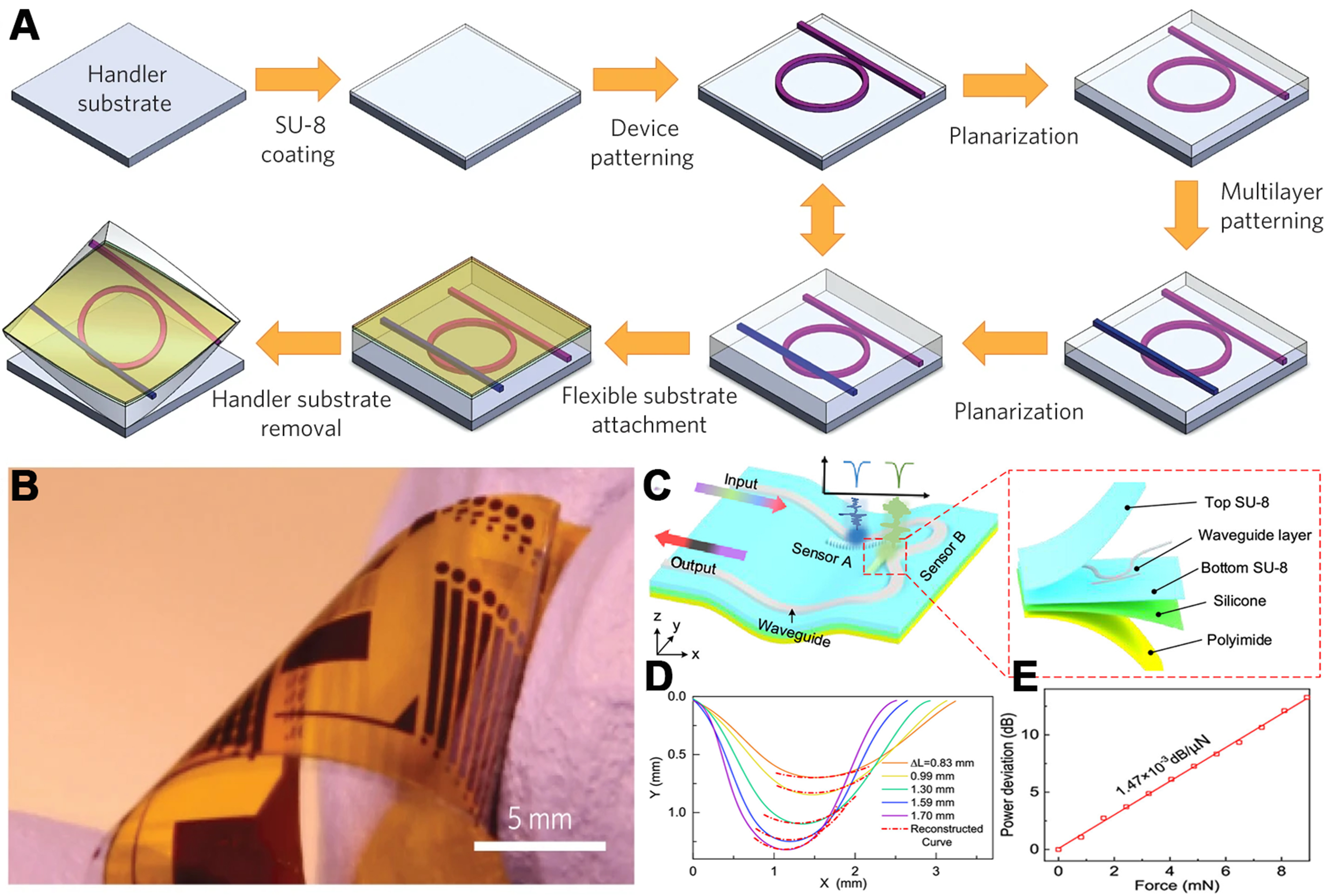
Figure 11. Flexible glass photonic device fabrication and applications[117]: (A) Schematic diagram of the device fabrication process; (B) Photograph of a flexible photonic chip. (A and B) are reprinted with permission from Ref.[117], Copyright © 2014 Springer Nature. Flexible ChG waveguide integrated strain sensors[105]: (C) Schematic of the flexible sensors; (D) Cross-sectional bending curves of the buckling chip under microscope observation (solid lines) and reconstructed by cascaded sensors (dotted lines) for different moving distances; (E) Relationship between the received optical power deviation and force applied on the sensor. (C-E) are reprinted with permission from Ref.[105], Copyright © 2023 American Chemical Society. ChG: Chalcogenide glass.
Another representative low-temperature deposition route is magnetron sputtering. For visible wavelength operation, common waveguide materials are TiO2 and SiN. While sputtered SiN has shown high performance at 1,550 nm, its implementation on flexible substrates and in the visible remains insufficiently explored. TiO2 can be deposited by e-beam evaporation and is widely used in metasurfaces[128,129], but its film density is typically lower than that of the sputtered films. Moreover, e-beam evaporated TiO2 often exhibits visible absorption due to oxygen loss during deposition. For sputtering-based TiO2, Chen et al. reported that reactive sputtering can damage flexible substrates via O2 plasma, resulting in poor optical film quality[113]. Chen et al. addressed this by introducing an ALD Al2O3 protection layer on the flexible substrate to block O2-plasma damage, enabling monolithic TiO2 photonic integration on flexible substrate[48] [Figure 12A]. At
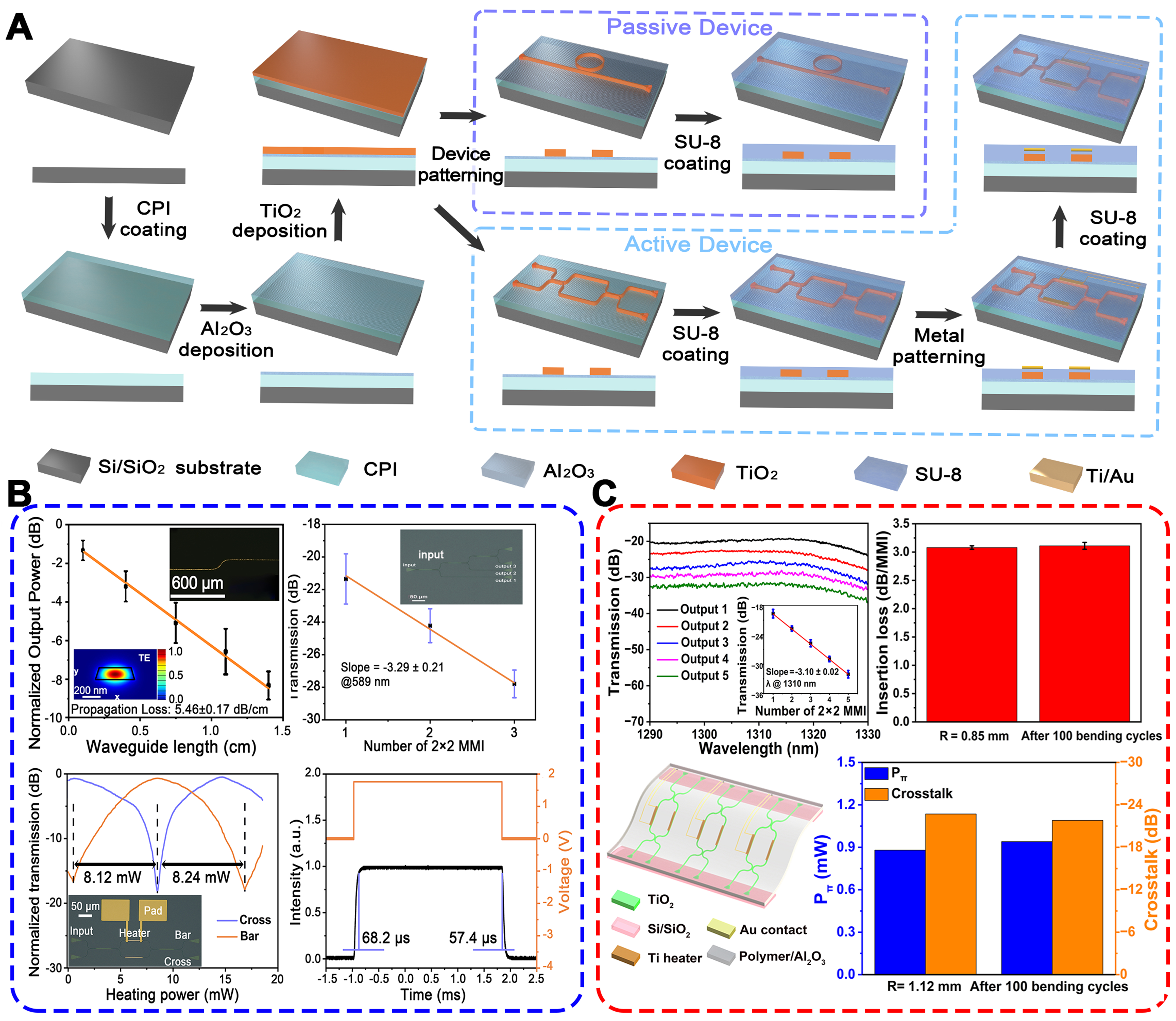
Figure 12. TiO2 integrated photonic monolithic integration process on flexible substrate[48]: (A) Schematic diagram of the device fabrication process. (B) TiO2 waveguide integrated devices at 589 nm: upper left: propagation loss; upper right: the insertion loss of 2 × 2 MMI; bottom left: the power of TOS; bottom right: the response time of TOS. (A and B) are reprinted with permission from Ref.[48], Copyright © 2025 Optica Publishing Group. (C) Flexible TiO2 waveguide integrated devices at 1,310 nm[57]: upper: Flexible 2 × 2 MMI measurement; bottom: Flexible TOS measurement. (C) is reprinted with permission from Ref.[57], Copyright © 2023 Optica Publishing Group. MMI: Multimode interference; TOS: thermo-optic switch; CPI: colorless polyimide; TE: transverse electric.
Development of flexible waveguide optogenetic probes
Although flexible integrated photonics with inorganic HIC waveguide cores has achieved multiple breakthroughs at both the process and device levels, flexible HIC waveguide optogenetic probes remain in their early stages of development. Most representative flexible waveguide-based optogenetic probes to date still rely on polymer waveguides[66,134-137]. This trend suggests that, in implantable probe formats, manufacturability, mechanical reliability, and optical transmission stability are currently more readily achieved with polymer-based implementations. These platforms offer favorable mechanical compliance and process compatibility, but their relatively low refractive index contrast limits compact routing, dense emitter integration, and scalable photonic network design. Therefore, existing polymer-based demonstrations should be viewed as important probe-level validations, whereas translating HIC-integrated waveguide architectures into flexible implantable optogenetic probes remains a key future direction.
This polymer-based route also highlights a central mechanical trade-off in flexible probe development. Although flexible probes can alleviate chronic mechanical mismatch between the probe and neural tissue after implantation, their low Young’s modulus and small geometrical dimensions often result in low bending stiffness during surgical insertion. When the tissue insertion force exceeds the critical buckling force of a flexible polymer probe, buckling or lateral deflection may occur, compromising implantation accuracy or even causing implantation failure, particularly for deep-brain targets. To address this trade-off, various implantation-assistance strategies have been developed, including polyethylene glycol (PEG)[138-140], silk[141,142], or other biodegradable stiffening coatings[143], as well as removable rigid insertion guides[144,145]. These approaches facilitate accurate delivery of flexible probes into target brain regions while preserving their low bending stiffness after implantation and reducing micromotion-induced tissue responses. In addition, optimizing the probe geometry to increase the critical buckling force at the insertion tip[134], without changing the material’s Young’s modulus, represents an effective strategy to reduce implantation difficulty. Chen et al. reported a flexible optogenetic stimulation probe built on a low-loss SU-8 polymer waveguide[134] [Figure 13A]. By optimizing the probe geometry [Figure 13B], they established a geometry–insertion model for the flexible probe. Within the defined structural design window, probes with a Young’s modulus close to that of SU-8 can achieve accurate assistance-free implantation, addressing the long-standing challenge of inserting flexible waveguide probes into deep brain regions without auxiliary tools [Figure 13C and D]. This strategy simplifies the implantation procedure while preserving the mechanical compliance of the polymer probe.
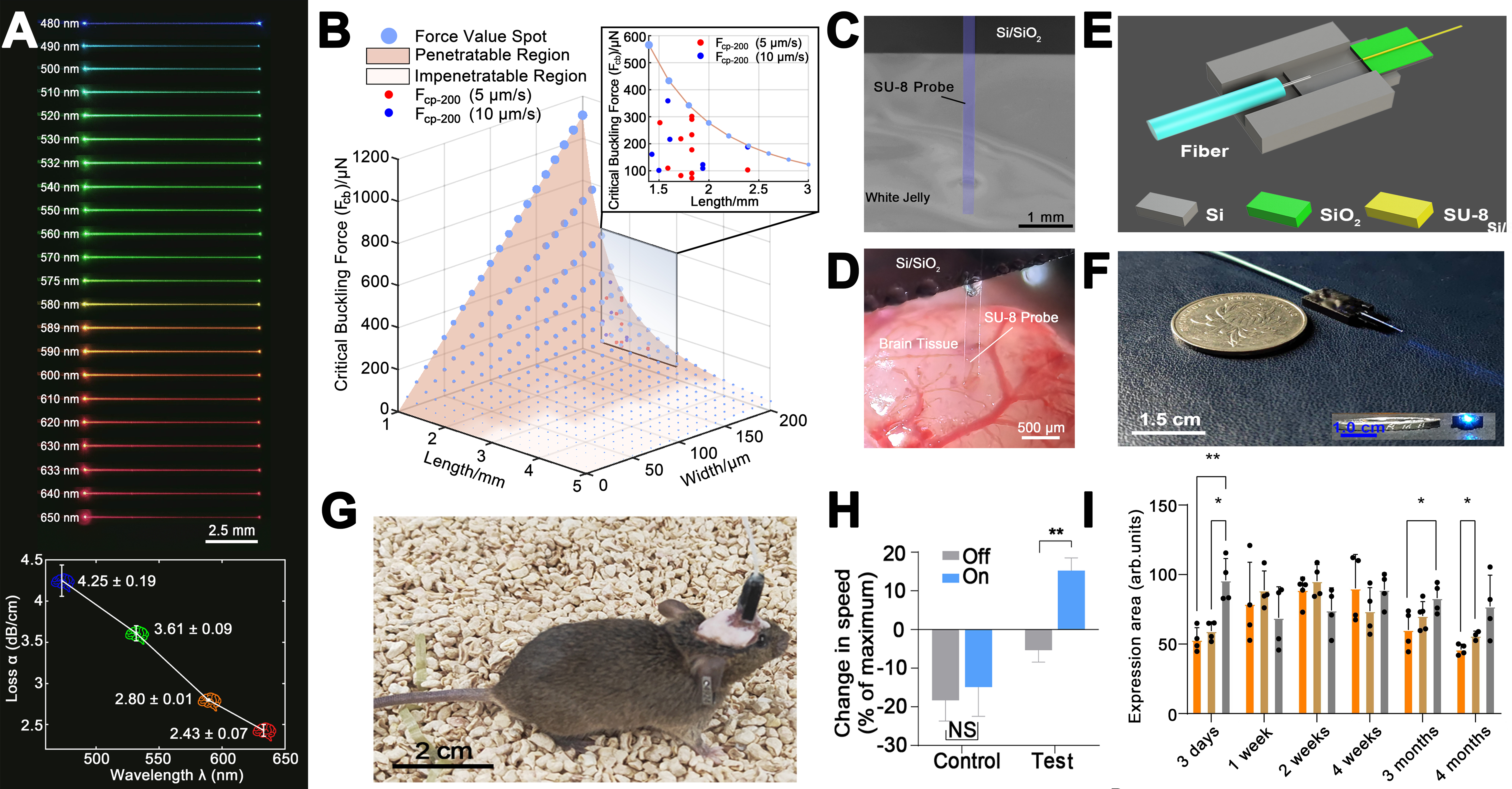
Figure 13. Flexible SU-8 waveguide optogenetic probe[134]: (A) the propagation loss of SU-8 waveguide at visible region; (B) Implant mechanical model with experimental data; Insertion of the flexible waveguide probe into the phantom brain (C) white jelly, (D) actual brain tissue; (E) Schematic diagram of packaging scheme; (F) Photograph of a well-encapsulated flexible waveguide probe; (G) Photograph of mice recovering from the probe implantation surgery; (H) Behavioral experiment; (I) Inflammatory experiment. NS is non-significance, meaning that there is no difference between the two groups. *P < 0.05, **P < 0.01. This figure is adapted from Ref.[134]. Copyright © 2024 Elsevier.
Optical packaging robustness is another critical requirement for translating flexible waveguide optogenetic probes toward long-term in vivo applications. At present, most waveguide-integrated probes still rely on fiber-coupled packaging[70,71,77,93,96], in which an optical fiber is aligned in a U- or V-groove[45,146], coupled to the on-chip waveguide, and fixed or shielded with ultraviolet (UV)-curable adhesives and black epoxy. Although this approach is simple and effective for benchtop testing or short-term validation, the fiber–chip coupling region remains a mechanically vulnerable joint in freely moving animals. Natural movement can mechanically stress this localized interface, leading to cracking, delamination, fiber misalignment, or breakage, ultimately resulting in coupling fluctuations or failure. Therefore, packaging robustness should be assessed not only by initial coupling efficiency but also by the long-term mechanical integrity and optical transmission stability of the fiber-waveguide interface under chronic implantation and free-moving conditions. To address this issue, Chen et al. proposed a more robust fiber-to-waveguide coupling and packaging scheme based on 3D-printed platform technology[134] [Figure 13E and F]. By fixing the jacketed external fiber and the probe onto a shared support platform, the optical coupling region is embedded within the package rather than being protected only by conventional point-wise adhesive bonding. This integrated encapsulation of the fiber–probe interface substantially improves fracture resistance and enables sustained optical stimulation sufficient for mouse locomotor speed modulation [Figure 13G and H], as well as a chronically low-inflammatory probe-tissue interface [Figure 13I]. However, real-time quantitative measurements of coupling-efficiency fluctuations during natural movement remain limited in this study and in most existing demonstrations of flexible waveguide optogenetic probes. Future work should therefore include pre- and post-implantation optical transmission measurements, bending or fatigue tests of the packaged coupling interface, accelerated soaking tests, and in vivo optical-output monitoring during freely moving behavior. From the perspective of mechano-optical coupling, the SU-8 probe represents a simplified single-polymer waveguide architecture, in which the absence of heterogeneous multilayer interfaces and phase-sensitive routing elements helps reduce deformation-induced coupling mismatch and phase drift during flexible implantation[8,147,148]. Taken together, this study should be viewed as a probe-level validation of flexible waveguide optogenetics under practical implantation and packaging constraints, showing that process-friendly polymer waveguides, when combined with robust packaging engineering and rapid assistance-free implantation, can close the essential validation loop from device fabrication to in vivo functional modulation. This provides application pull for future probes with higher channel counts and more complex integrated waveguide architectures, including hybrid HIC platforms such as TiO2 waveguide cores embedded in SU-8 claddings for flexible optoelectronic optogenetic probes.
In conventional polymer waveguide probes, optical emission typically follows the waveguide’s axial direction of the waveguide because these devices often rely on end-fire emission from the waveguide terminal, lacking integrated out-of-plane coupling structures to redirect light toward the surrounding tissue. As a result, light propagates along the probe shank, which can reduce spatial localization and increase overlap between the optical path and recording electrodes or nearby interconnects, thereby increasing the risk of undesired illumination and photoelectric recording artifacts caused by the visible-light response of metal electrodes[149-152] [Figure 14A]. To address this emission-direction problem, Reddy et al. introduced a Parylene C/PDMS flexible waveguide platform with integrated 45° micro-reflectors, which redirected the guided light into vertical out-of-plane emission[66] [Figure 14B and C]. This built-in micro-mirror out-coupling enables light delivery normal to the probe surface, thereby addressing a recurring limitation of axial end-fire emission by reducing overlap between the optical path and electrode layout [Figure 14A], minimizing undesired illumination and optical artifacts, and preserving a planar architecture compatible with electrophysiological integration. The platform was subsequently combined with tungsten electrodes to achieve in vivo optical stimulation with concurrent electrophysiological recording[137]. Thus, it demonstrates a scalable interface form factor based on flexible waveguide arrays with on-chip vertical out-couplers and supports the rationale of using vertically emitting grating couplers on HIC waveguide platforms for out-of-plane delivery. In addition, the Parylene C/PDMS platform also reflects a neutral-axis design principle: the Parylene C waveguide is positioned near the geometric center between the upper and lower PDMS cladding layers, which helps reduce bending-induced strain in the optical layer. By contrast, the local multiple-neutral-axis strategy summarized in Figure 9 has so far been demonstrated mainly in general flexible photonic devices and has not yet been fully translated into flexible waveguide optogenetic probes. Nevertheless, with continued advances in fabrication processes and device-level co-design, this strategy provides a promising mechanical framework for future multilayer HIC optogenetic probes that integrate inorganic waveguide cores, electrodes, heaters, and encapsulation layers.
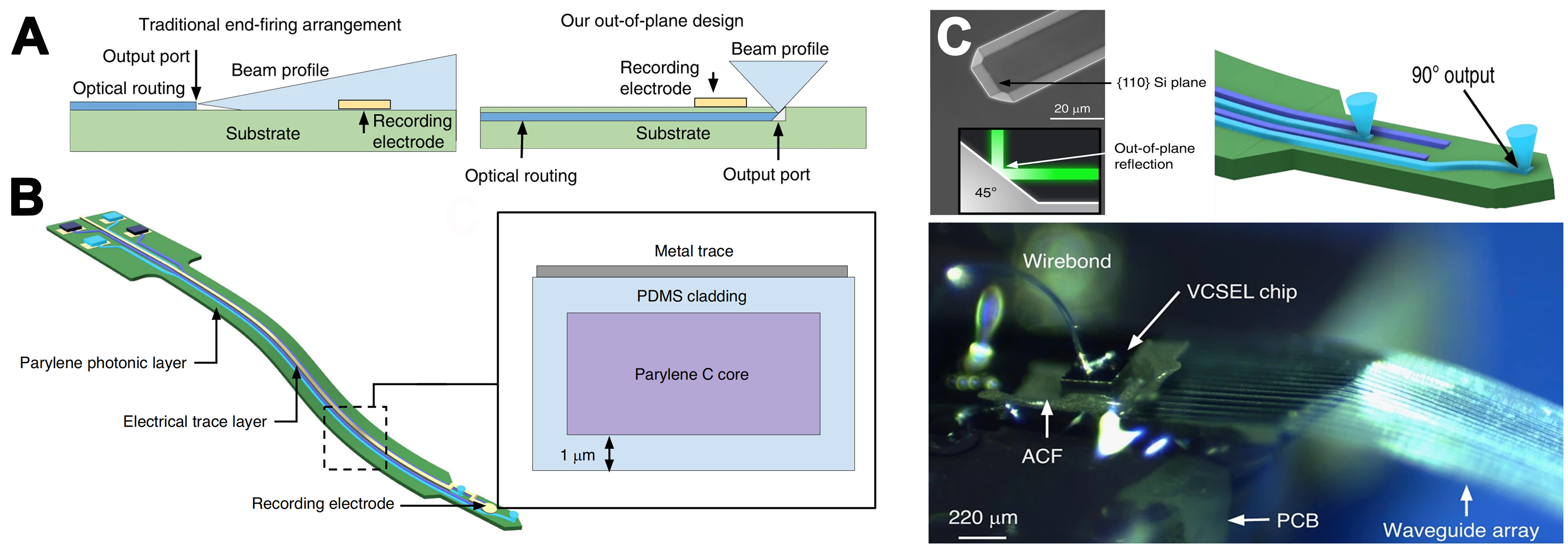
Figure 14. Flexible Parylene C waveguide optogenetic probe[66]: (A) Schematic of the traditional in-plane/out-of-plane illumination from an end-firing waveguide; (B) A conceptual schematic of a Parylene photonic waveguide neural probe with a 45° aluminum reflector; (C) Photograph of flexible Parylene waveguide array with a bonded VCSEL chip. This figure is adapted from Ref.[66]. Copyright © 2020 The Author(s). VCSEL: Vertical-cavity surface-emitting laser; PDMS: polydimethylsiloxane; ACF: anisotropic conductive film; PCB: printed circuit board.
Overall, flexible optogenetic waveguide probes remain largely polymer-based, whereas reports of flexible integrated probes built on inorganic high-index waveguides (e.g, SiN/SiON/TiO2) are still relatively scarce, largely because manufacturability, mechanical reliability, and low-loss routing waveguides are difficult to satisfy simultaneously. Inorganic thin films are typically more sensitive to deposition temperature, residual stress, and etch/plasma processes. After transferring to compliant substrates, they are prone to warpage, cracking, and interfacial delamination, which degrade propagation loss and device uniformity. Meanwhile, flexible substrates generally exhibit poorer surface planarity than rigid wafers[153], substantially narrowing the process window for stepper-based or scanner-based lithography. Focus drift readily induces critical-dimension errors and pattern distortion. In addition, the low electrical and thermal conductivity of flexible substrates makes wafer-scale control of film uniformity/density and etch uniformity/etch-depth accuracy more challenging, further amplifying channel-to-channel variation and network-level errors. Despite recent advances in flexible waveguide-integrated routes, substantial engineering barriers remain for wafer-scale, reproducible manufacturing. Consequently, at the current probe validation stage, polymer waveguides enabled by low-temperature processing, the coupling tolerance of thicker cores, packaging compatibility, and mechanical compliance, more readily achieve multi-channel light delivery with chronic usability, leading to a field landscape in which flexible waveguide optogenetic probes are polymer-dominant, with inorganic core approaches promising but still awaiting key breakthroughs.
CONCLUSION AND OUTLOOK
This review centers on integrated optical routing waveguides for optogenetic probes, systematically summarizing the underlying routing physics, implementation paradigms on rigid platforms, and the coupled materials-mechanics-process constraints that emerge when transitioning to flexible platforms. Overall, waveguide routing elevates optogenetic probes from active-source-placement or fiber-delivery-driven point illumination to a networked optical distribution system defined by topology and weights, offering a clear path toward scalable, programmable, high-resolution addressing across multiple depths and brain regions. At the same time, flexibility makes bending and micromotion routine perturbations under chronic in vivo conditions, shifting the determinants of routing performance from single-device metrics to system-level coupled constraints spanning phase/coupling stability, packaging/interconnect reliability, and manufacturing uniformity. Building on this framework, we outline future directions in five areas: materials and device scaling, multimodal system capability, on-probe light-source integration, manufacturing and process maturation, and platform transferability.
Toward flexible HIC waveguide routing with dense, independently addressable sites
As neuroscience shifts from region-level modulation to causal interrogation at the ensemble and even single-cell scales, experimental demands for multi-region, multi-depth, high spatiotemporal-resolution control will continue to intensify[154,155]. This trend fundamentally drives on-shank photonic routing toward higher channel counts and tighter port-to-port uniformity within stringent shank area constraints. While flexible hybrid platforms (inorganic core/organic cladding) promise compactness and scalability, their probe-grade translation is gated by stress management, interfacial reliability, and wafer-scale uniformity. Against this backdrop, coherence-enabled wavefront engineering - including optical phased arrays and coherent multi-port synthesis - offers an alternative scaling axis: it can shift the paradigm from “one channel–one fixed emission site/pattern” to “one channel–programmable beam steering and volumetric scanning”, thereby increasing per-channel spatial interrogability without a linear increase in physical output ports[156-159]. Under in vivo conditions characterized by deep targets, strong scattering, and tight thermal budgets, this approach may also open a more favorable system-level trade space among port count, footprint, and power, making it a promising route toward scalable, high-density optogenetic probes.
Multimodal closed-loop neural interfaces based on waveguide routing
Building on high-density, addressable optical stimulation, the next scientifically impactful direction is to co-integrate high-throughput electrophysiological recording with chemical/environmental sensing to form a multimodal interface on a single implant[128]. The key advance is not a simple “more channels” stack-up, but a shift from open-loop to closed-loop neuromodulation: electrical signals provide fast dynamic readout, while chemical and environmental variables (e.g., local metabolism, inflammation-related markers, temperature, and micro-environmental changes) supply slow and state variables, enabling causal dissection of state-dependent circuit function, neuromodulatory mechanisms, and long-term plasticity[16,160,161]. From a system perspective, the optical routing waveguide network can serve as the implant’s “photonic backbone”, but it must be co-designed with electrode layout, sensing interfaces, packaging, and thermal budget to prevent crosstalk and long-term drift.
Integrated light sources on flexible waveguide probes
Current flexible waveguide optogenetic systems still predominantly rely on fiber-coupled external light sources, which are robust and readily scalable for laboratory validation but impose inherent constraints for freely moving experiments, chronic implantation, and system miniaturization. For next-generation platforms, the central challenge is efficient on-chip light source integration on the flexible substrate. Heterogeneous integration of III-V lasers, μ-LEDs, micro-organic light-emitting diodes (μ-OLEDs), or other microscale emitters has become an important route toward compact, scalable, and fully integrated photonic platforms[162-164]. These approaches indicate that light sources can, in principle, be incorporated into miniaturized photonic or neural-interface platforms rather than being supplied exclusively through external fibers.
For flexible waveguide optogenetic probes, the potential of integrated light sources lies not only in eliminating external fiber coupling, but also in converting a passive optical delivery probe into an active optoelectronic information interface[165]. Source integration would allow electrical control signals to be directly converted into programmable optical outputs on the probe, including intensity modulation[166], pulse-pattern control[166] and multi-wavelength operation[18,97]. When combined with on-probe waveguide routing, these electrically programmable light sources could provide temporal and spectral degrees of freedom[97], while the waveguide network defines spatial light delivery across multiple stimulation sites[35]. More importantly, co-integration with the aforementioned multimodal platform could support wholly closed-loop optoelectronic operation[167], in which recorded neural or physiological signals are processed as feedback, translated into programmed optical stimulation, and monitored through the same multimodal interface. In this sense, heterogeneous light-source integration could transform flexible waveguide optogenetic probes from externally driven light delivery tools into miniaturized, fiber-free, and feedback-capable neural-interface systems.
Despite these potential advantages, translating heterogeneous light-source integration into flexible waveguide optogenetic probes remains substantially more challenging. First, the interface between the light source and the flexible waveguide must be tightly and reliably bonded to prevent interfacial cracking during long-term operation, which could otherwise lead to optical coupling failure. Second, integrating light sources onto the probe introduces local power-delivery and heat-dissipation requirements. Therefore, electrical and thermal crosstalk within the system must be carefully optimized to avoid interference with electrophysiological signals. Finally, the entire source–waveguide–electrode stack requires mechanically robust and water-barrier packaging to survive long-term implantation without delamination, corrosion, or mechanically induced optical drift.
Manufacturing: bridging lab innovation and foundry-scale reproducibility
To support multi-channel routing waveguides and multimodal integration, flexible photonics manufacturing must advance from one-off feasibility to repeatable, scalable fabrication. At the laboratory stage, this still requires developing low-temperature, low-stress deposition methods, new patterning methods, and packaging/interconnect processes to rapidly iterate on material stacks and device architectures. Longer-term and more decisive collaboration with foundries is needed to establish manufacturable process modules and PDKs for flexible/peeling-off/transferable platforms, while integrating stress windows, yield statistics, device uniformity, and system-level testing into a unified flow. For routing waveguide networks, such “foundry-ready” capability directly sets port-to-port consistency, loss budgets, and the ceiling for scalable expansion.
From optogenetic waveguide probes to a general bio-integrated photonic platform
Although this review focuses on flexible waveguide-integrated optogenetic probes for brain research, its longer-term value lies in its transferability as a platform for bio-integrated photonics. Once a stable technology stack is established, spanning flexible HIC routing waveguides, multimodal integration, packaging/interconnects, and reproducible manufacturing-the platform can be translated more rapidly and efficiently to applications, such as spinal cord[168,169] and peripheral nerve[170] modulation, cardiac electrophysiology with optical actuation[171,172], and multi-site stimulation/readout in organoid and tissue-engineering models[173,174]. This shift from “application-specific devices” to a “platform technology stack” will mark a key step in advancing flexible photonic neural interfaces from laboratory tools toward scalable bio-integrated technologies.
In conclusion, integrated optical routing is emerging as a unifying design paradigm for next-generation optogenetic probes, because it reframes neural illumination from a “active source placement” and “fiber delivery” task into a scalable problem of photonic-network distribution and programmability. Rigid platforms have established the geometric precision and reconfigurability of routing architectures, whereas flexible platforms further highlight that, under chronic in vivo conditions, routing fidelity is ultimately governed by the coupled effects of mechanical perturbations, material systems, and manufacturability. Looking ahead, HIC flexible waveguides, multimodal closed-loop integration, efficient on-chip light sources and power delivery, and foundry-aligned wafer-scale manufacturing will together determine whether flexible integrated photonic optogenetic probes can progress from laboratory demonstrations to high-channel-count, long-term bio-integrated systems. The resulting platform could extend beyond neuroscience, enabling quasi-distributed optical actuation and sensing across diverse bio-interfaces.
DECLARATIONS
Authors’ contributions
Conceptualization: Chen, Z.; Li, L.
Writing: Chen, Z.; Tang, Y.
Project assistance: Zhang, S.; Li, X.; Li, H.; Zhao, W.; Zou, S.; Lin, H.; Gong, W.; Si, K.
Review and editing, supervision, project administration: Li, L.
Availability of data and materials
Not applicable.
AI and AI-assisted tools statement
During the preparation of this manuscript, the AI tool ChatGPT (OpenAI, GPT-5.3) was used solely for language polishing and readability improvement. The tool did not influence the literature selection, interpretation, or scientific content of the work. All authors take full responsibility for the accuracy, integrity, and final content of the manuscript.
Financial support and sponsorship
This work was supported by the Key R&D Program of Zhejiang Province (2024C03150, 2025C01119, 2025C01002), “Pioneer” and “Leading Goose” R&D Program of Zhejiang Province (2024SDXHDX0005), STI 2030-Major Projects (2021ZD0200401), the Key Project of Westlake Institute for Optoelectronics (Grant No. 2024GD002 received by Lin, H.), and Fundamental Research Funds for the Central Universities.
Conflicts of interest
All authors declared that there are no conflicts of interest.
Ethical approval and consent to participate
Not applicable.
Consent for publication
Not applicable.
Copyright
© The Author(s) 2026.
REFERENCES
1. Moreaux, L. C.; Yatsenko, D.; Sacher, W. D.; et al. Integrated neurophotonics: toward dense volumetric interrogation of brain circuit activity-at depth and in real time. Neuron 2020, 108, 66-92.
2. Zhao, H.; Yue, H.; Chou, W.; et al. Optogenetic technology: breakthroughs and challenges from basic research to clinical translation. Adv. Photon. 2025, 7, 054001.
3. Lu, Q.; Sun, Y.; Liang, Z.; Zhang, Y.; Wang, Z.; Mei, Q. Nano-optogenetics for disease therapies. ACS. Nano. 2024, 18, 14123-44.
4. Zhang, Q.; Li, T.; Xu, M.; Islam, B.; Wang, J. Application of optogenetics in neurodegenerative diseases. Cell. Mol. Neurobiol. 2024, 44, 57.
5. Kim, J.; Gilbert, E.; Arndt, K.; et al. Multifunctional tetrode-like drug delivery, optical stimulation, and electrophysiology (Tetro-DOpE) probes. Biosens. Bioelectron. 2024, 265, 116696.
6. Jiang, S.; Patel, D. C.; Kim, J.; et al. Spatially expandable fiber-based probes as a multifunctional deep brain interface. Nat. Commun. 2020, 11, 6115.
7. Park, S.; Yuk, H.; Zhao, R.; et al. Adaptive and multifunctional hydrogel hybrid probes for long-term sensing and modulation of neural activity. Nat. Commun. 2021, 12, 3435.
8. Huang, S.; Liu, X.; Lin, S.; et al. Control of polymers’ amorphous-crystalline transition enables miniaturization and multifunctional integration for hydrogel bioelectronics. Nat. Commun. 2024, 15, 3525.
9. Spagnolo, B.; Balena, A.; Peixoto, R. T.; et al. Tapered fibertrodes for optoelectrical neural interfacing in small brain volumes with reduced artefacts. Nat. Mater. 2022, 21, 826-35.
10. Sahasrabudhe, A.; Rupprecht, L. E.; Orguc, S.; et al. Multifunctional microelectronic fibers enable wireless modulation of gut and brain neural circuits. Nat. Biotechnol. 2024, 42, 892-904.
11. Sparta, D. R.; Stamatakis, A. M.; Phillips, J. L.; Hovelsø, N.; van Zessen, R.; Stuber, G. D. Construction of implantable optical fibers for long-term optogenetic manipulation of neural circuits. Nat. Protoc. 2011, 7, 12-23.
12. Mohit, F.; Ricciardi, A.; Cusano, A.; Cutolo, A. Tapered multicore optical fiber probe for optogenetics. Results. Opt. 2021, 4, 100109.
13. Du, Y.; Turtaev, S.; Leite, I. T.; et al. Hybrid multimode - multicore fibre based holographic endoscope for deep-tissue neurophotonics. Light. Adv. Manuf. 2022, 3, 408-16.
14. Pisanello, F.; Sileo, L.; Oldenburg, I. A.; et al. Multipoint-emitting optical fibers for spatially addressable in vivo optogenetics. Neuron 2014, 82, 1245-54.
15. Packer, A. M.; Russell, L. E.; Dalgleish, H. W.; Häusser, M. Simultaneous all-optical manipulation and recording of neural circuit activity with cellular resolution in vivo. Nat. Methods. 2015, 12, 140-6.
16. Kim, T. I.; McCall, J. G.; Jung, Y. H.; et al. Injectable, cellular-scale optoelectronics with applications for wireless optogenetics. Science 2013, 340, 211-6.
17. Gu, W.; Wang, L.; Wang, X.; Zhao, C.; Guan, S. Large-scale, high-density microLED array-based optogenetic device for neural stimulation and recording. Nano. Lett. 2024, 24, 15252-9.
18. Li, L.; Lu, L.; Ren, Y.; et al. Colocalized, bidirectional optogenetic modulations in freely behaving mice with a wireless dual-color optoelectronic probe. Nat. Commun. 2022, 13, 839.
19. Stujenske, J. M.; Spellman, T.; Gordon, J. A. Modeling the spatiotemporal dynamics of light and heat propagation for in vivo optogenetics. Cell. Rep. 2015, 12, 525-34.
20. Lin, R.; Guo, J.; Tong, J.; et al. Treatment of neuropathic pain after brachial plexus injury by implantable wireless charging flexible micro-LED array. Opt. Express. 2025, 33, 31819-31.
21. Cai, X.; Zhang, H.; Wei, P.; et al. A wireless optoelectronic probe to monitor oxygenation in deep brain tissue. Nat. Photon. 2024, 18, 492-500.
22. Greer, R.; Verdier, A.; Butt, E.; et al. Chronically implantable μLED arrays for optogenetic cortical surface stimulation in mice. Nat. Commun. 2026, 17, 878.
23. Yang, Y.; Wu, M.; Vázquez-Guardado, A.; et al. Wireless multilateral devices for optogenetic studies of individual and social behaviors. Nat. Neurosci. 2021, 24, 1035-45.
24. Wu, M.; Yang, Y.; Zhang, J.; et al. Patterned wireless transcranial optogenetics generates artificial perception. Nat. Neurosci. 2026, 29, 234-45.
25. Vöröslakos, M.; Kim, K.; Slager, N.; et al. HectoSTAR μLED optoelectrodes for large-scale, high-precision in vivo opto-electrophysiology. Adv. Sci. 2022, 9, e2105414.
26. Lu, J.; Zia, M.; Baig, D. A.; et al. Opto-myomatrix: μLED integrated microelectrode arrays for optogenetic activation and electrical recording in muscle tissue. bioRxiv 2025.
27. Wan, Y.; He, W.; Jaussi, J.; et al. Integrating silicon photonics with complementary metal–oxide–semiconductor technologies. Nat. Rev. Electr. Eng. 2026, 3, 15-31.
28. Ma, X.; Yuan, M.; Li, J.; et al. Multi-target and ultra-high-speed optical wireless communication using a thin-film lithium niobate optical phased array. Nat. Commun. 2025, 17, 969.
29. Zheng, Y.; Wang, H.; Jia, X.; et al. Large-scale quantum communication networks with integrated photonics. Nature 2026, 651, 68-75.
30. Lin, H.; Zheng, H.; Zhu, W.; et al. Multifunctional lithium niobate platform for photodetection and photoacoustic and thermoelastic gas sensing. Nat. Commun. 2026, 17, 2296.
31. Zhang, S.; Jiang, X.; Wu, B.; et al. Photonic edge intelligence chip for multi-modal sensing, inference and learning. Nat. Commun. 2025, 16, 10136.
32. Al-Kayed, N.; St-Arnault, C.; Morison, H.; et al. Programmable 200 GOPS Hopfield-inspired photonic Ising machine. Nature 2025, 648, 576-84.
33. Ashtiani, F.; Idjadi, M. H.; Kim, K. Integrated photonic neural network with on-chip backpropagation training. Nature 2026, 651, 927-32.
34. Yeh, S. K.; Shih, C. T.; Yuan, F.; et al. Silicon photonics platform for next generation data communication technologies. In Proceedings of the 2024 IEEE International Electron Devices Meeting (IEDM), San Francisco, USA. Dec 7-11, 2024. IEEE; 2024. p. 1-4.
35. Mohanty, A.; Li, Q.; Tadayon, M. A.; et al. Reconfigurable nanophotonic silicon probes for sub-millisecond deep-brain optical stimulation. Nat. Biomed. Eng. 2020, 4, 223-31.
36. Sacher, W. D.; Chen, F. D.; Moradi-Chameh, H.; et al. Optical phased array neural probes for beam-steering in brain tissue. Opt. Lett. 2022, 47, 1073-6.
37. Lakunina, A. A.; Socha, K. Z.; Ladd, A. E.; et al. Neuropixels Opto: combining high-resolution electrophysiology and optogenetics. Nat. Methods. 2026, 23, 1207-16.
38. Lv, S.; Xu, Z.; Mo, F.; et al. Long-term stability strategies of deep brain flexible neural interface. npj. Flex. Electron. 2025, 9, 410.
39. Wang, S.; Jiang, Q.; Liu, H.; et al. Mechanically adaptive and deployable intracortical probes enable long-term neural electrophysiological recordings. Proc. Natl. Acad. Sci. U. S. A. 2024, 121, e2403380121.
40. Hayati Raad, S. Perspective chapter: Optical waveguides for quantum computation. In Optical waveguide technology and and applications. Kim, K.Y., Ed.; IntechOpen: London, 2024.
41. Okamoto, K. Chapter 2 - Planar optical waveguides. In Fundamentals of optical waveguides (third edition). Academic Press: 2022; pp. 13-65.
42. Hammer, M.; Khan, S. S.; Taheri, B.; Farheen, H.; Förstner, J. TFLN channel waveguides of rib and strip type: properties of guided modes. Opt. Continuum. 2025, 4, 2356.
43. Aharonovich, I.; Crozier, K. B.; Neshev, D. Programmable integrated quantum photonics. Nat. Photon. 2026, 20, 254-65.
44. Hu, Y.; Song, Y.; Zhu, X.; et al. Integrated lithium niobate photonic computing circuit based on efficient and high-speed electro-optic conversion. Nat. Commun. 2025, 16, 8178.
45. Son, Y.; Lee, H. J.; Kim, J.; et al. In vivo optical modulation of neural signals using monolithically integrated two-dimensional neural probe arrays. Sci. Rep. 2015, 5, 15466.
46. Sacher, W. D.; Luo, X.; Yang, Y.; et al. Visible-light silicon nitride waveguide devices and implantable neurophotonic probes on thinned 200 mm silicon wafers. Opt. Express. 2019, 27, 37400-18.
47. Luo, Y.; Sun, C.; Ma, H.; et al. Flexible passive integrated photonic devices with superior optical and mechanical performance. Opt. Express. 2022, 30, 26534-43.
48. Chen, Z.; Tang, Y.; Wei, M.; et al. Development of yellow-light TiO2 integrated photonics. Opt. Lett. 2025, 50, 3489-92.
49. Krutov, I. A.; Saygin, M. Y.; Dyakonov, I. V.; Kulik, S. P. Optimized low-loss integrated photonics silicon-nitride Y-branch splitter. AIP. Conf. Proc. 2020, 2241, 020027.
50. Kobayashi, M. Chapter 10 - Guided-wave optical interconnect techniques. In Photonics in switching. Academic Press: 1993; pp. 271-317.
51. Sahu, P. P. Multimode interference coupler based on general interference for integrated optical and quantum optic devices: a review. Phys. Scr. 2024, 99, 085106.
52. Wu, Y.; Wu, M.; Vázquez-Guardado, A.; et al. Wireless multi-lateral optofluidic microsystems for real-time programmable optogenetics and photopharmacology. Nat. Commun. 2022, 13, 5571.
53. Peng, Y.; Zhao, W.; Shi, Y.; Dai, D. 192-channel silicon reconfigurable optical add-drop multiplexer. In Proceedings of the 2024 IEEE Silicon Photonics Conference (SiPhotonics), Tokyo, Japan. Apr 15-18, 2024. IEEE; 2024. p. 1-2.
54. Xia, D.; Luo, L.; Wang, L.; et al. Reconfigurable chalcogenide integrated nonlinear photonics. Nat. Commun. 2025, 16, 10133.
55. Gurses, V.; Davis, S. I.; Valivarthi, R.; Sinclair, N.; Spiropulu, M.; Hajimiri, A. An on-chip phased array for non-classical light. Nat. Commun. 2025, 16, 6849.
56. Liang, G.; Huang, H.; Mohanty, A.; et al. Robust, efficient, micrometre-scale phase modulators at visible wavelengths. Nat. Photon. 2021, 15, 908-13.
57. Chen, Z.; Wei, M.; Sun, B.; et al. Flexible waveguide integrated thermo-optic switch based on TiO2 platform. Opt. Lett. 2023, 48, 3239-42.
58. Frigg, A.; Boes, A.; Ren, G.; et al. Low loss CMOS-compatible silicon nitride photonics utilizing reactive sputtered thin films. Opt. Express. 2019, 27, 37795-805.
59. Guha, B.; Cardenas, J.; Lipson, M. Athermal silicon microring resonators with titanium oxide cladding. Opt. Express. 2013, 21, 26557-63.
60. Park, H.; Jung, J.; Zhang, Y.; et al. Effects of thermally induced phase transition on the negative thermo-optic properties of atomic-layer-deposited TiO2 films. ACS. Appl. Electron. Mater. 2022, 4, 651-62.
61. Reshef, O.; Shtyrkova, K.; Moebius, M. G.; et al. Polycrystalline anatase titanium dioxide microring resonators with negative thermo-optic coefficient. J. Opt. Soc. Am. B. 2015, 32, 2288.
62. West, G. N.; Loh, W.; Kharas, D.; et al. Low-loss integrated photonics for the blue and ultraviolet regime. APL. Photonics. 2019, 4, 026101.
63. Sorace-Agaskar, C.; Kharas, D.; Yegnanarayanan, S.; et al. Versatile silicon nitride and alumina integrated photonic platforms for the ultraviolet to short-wave infrared. IEEE. J. Select. Topics. Quantum. Electron. 2019, 25, 1-15.
64. Zhong, C.; Ma, H.; Sun, C.; et al. Fast thermo-optical modulators with doped-silicon heaters operating at 2 μm. Opt. Express. 2021, 29, 23508-16.
65. Lin, X.; Ling, T.; Subbaraman, H.; Guo, L. J.; Chen, R. T. Printable thermo-optic polymer switches utilizing imprinting and ink-jet printing. Opt. Express. 2013, 21, 2110-7.
66. Reddy, J. W.; Lassiter, M.; Chamanzar, M. Parylene photonics: a flexible, broadband optical waveguide platform with integrated micromirrors for biointerfaces. Microsyst. Nanoeng. 2020, 6, 85.
67. Sun, Y.; Wang, D.; Niu, H.; et al. Programmable photonic processors with MZI-cascaded-ring units for enhanced versatility. Photon. Res. 2025, 13, 2778.
68. Marchisio, A.; Da Ros, F.; Curri, V.; Carena, A.; Bardella, P. Comprehensive model of MZI-based circuits for photonic computing applications. Commun. Phys. 2025, 8, 2176.
69. Sun, C.; Chen, Z.; Ye, Y.; et al. Integrated microring spectrometer with in‐hardware compressed sensing to break the resolution‐bandwidth limit for general continuous spectrum analysis. Laser. Photonics. Rev. 2023, 17, 2300291.
70. Chen, F.; Chameh, H. M.; Movahed, M.; et al. Implantable nanophotonic neural probes for integrated patterned photostimulation and electrophysiological recording. npj. Biosensing. 2025, 2, 24.
71. Chen, F. D.; Sharma, A.; Xue, T.; et al. Implantable silicon neural probes with nanophotonic phased arrays for single-lobe beam steering. Commun. Eng. 2024, 3, 182.
72. Marchetti, R.; Lacava, C.; Carroll, L.; Gradkowski, K.; Minzioni, P. Coupling strategies for silicon photonics integrated chips [Invited]. Photon. Res. 2019, 7, 201.
73. Xue, T.; Stalmashonak, A.; Chen, F. D.; et al. Implantable photonic neural probes with out-of-plane focusing grating emitters. Sci. Rep. 2024, 14, 13812.
74. Segev, E.; Reimer, J.; Moreaux, L. C.; et al. Patterned photostimulation via visible-wavelength photonic probes for deep brain optogenetics. Neurophotonics 2017, 4, 011002.
75. Li, L.; Lin, H.; Qiao, S.; et al. Monolithically integrated stretchable photonics. Light. Sci. Appl. 2018, 7, 17138.
76. Chen, Z.; Li, L. Flexible photonic probes for new-generation brain–computer interfaces. Acc. Mater. Res. 2021, 2, 315-8.
77. Mu, X.; Chameh, H. M.; Movahed, M.; et al. Nanophotonic neural probes for in vivo photostimulation, electrophysiology, and microfluidic delivery. Microsyst. Nanoeng. 2026, 12, 100.
78. Yu, X.; Wu, Z.; Zeng, J.; Lin, S.; Cai, X.; Zhang, Y. 532 nm silicon nitride optical phased array and high-speed calibration and control system. Chin. Opt. Lett. 2025, 23, 061301.
79. Chul Shin, M.; Mohanty, A.; Watson, K.; et al. Chip-scale blue light phased array. Opt. Lett. 2020, 45, 1934-7.
80. Poulton, C. V.; Byrd, M. J.; Raval, M.; et al. Large-scale silicon nitride nanophotonic phased arrays at infrared and visible wavelengths. Opt. Lett. 2017, 42, 21-4.
81. McKay, E.; Pruiti, N. G.; May, S.; Sorel, M. High-confinement alumina waveguides with sub-dB/cm propagation losses at 450 nm. Sci. Rep. 2023, 13, 19917.
82. Hegeman, I.; Dijkstra, M.; García-Blanco, S. M. Low loss TiO2 channel waveguides. In Proceedings of the Integrated Optics: Devices, Materials, and Technologies XXIV, 2020.
83. Hegeman, I.; Dijkstra, M.; Segerink, F. B.; Lee, W.; Garcia-Blanco, S. M. Development of low-loss TiO2 waveguides. Opt. Express. 2020, 28, 5982-90.
84. Evans, C. C.; Liu, C.; Suntivich, J. Low-loss titanium dioxide waveguides and resonators using a dielectric lift-off fabrication process. Opt. Express. 2015, 23, 11160-9.
85. Corato-Zanarella, M.; Ji, X.; Mohanty, A.; Lipson, M. Absorption and scattering limits of silicon nitride integrated photonics in the visible spectrum. Opt. Express. 2024, 32, 5718-28.
86. Zhou, D.; Callori, G.; Vereecke, B.; et al. A 300mm silicon nitride photonic platform for ultra low loss in the visible spectrum. In Proceedings of the 2024 International Conference on Optical MEMS and Nanophotonics (OMN), San Sebastian, Spain. July 28 - Aug 01, 2024. IEEE; 2024. p. 1-2.
87. Shi, B.; Zheng, M. Y.; Hu, Y.; et al. A hyperfine-transition-referenced vector spectrum analyzer for visible-light integrated photonics. Nat. Commun. 2025, 16, 7025.
88. Yang, S.; Ding, Z.; Li, X.; et al. Visible to near-infrared light integrated photonic components on PECVD and LPCVD SiN platform. IEEE. Photonics. J. 2024, 16, 1-7.
89. Neutens, P.; Mafakheri, E.; Zheng, X.; et al. A 200 mm wafer-scale Al2O3 photonics waveguide technology for UV and visible applications. IEEE. Photonics. J. 2025, 17, 1-6.
90. Dullo, F. T.; Jayakumar, N.; Getz, M.; et al. Low-loss, low-background aluminum oxide waveguide platform for broad-spectrum on-chip microscopy. Opt. Lett. 2025, 50, 2159-62.
91. Yamaguchi, T.; Fushimi, N.; Hida, M.; et al. Optical waveguides and beam splitters using low-loss aluminum oxide for visible-wavelength photonics applications. Jpn. J. Appl. Phys. 2025, 64, 02SP32.
92. Shim, E.; Chen, Y.; Masmanidis, S.; Li, M. Multisite silicon neural probes with integrated silicon nitride waveguides and gratings for optogenetic applications. Sci. Rep. 2016, 6, 22693.
93. Lanzio, V.; Telian, G.; Koshelev, A.; et al. Small footprint optoelectrodes using ring resonators for passive light localization. Microsyst. Nanoeng. 2021, 7, 40.
94. Fu, T.; Zhang, J.; Sun, R.; et al. Optical neural networks: progress and challenges. Light. Sci. Appl. 2024, 13, 263.
95. Lin, S.; Zeng, J.; Lin, S.; Yu, S.; Zhang, Y. High-fidelity and compact topology architecture for large-scale reconfigurable linear optical networks. Adv. Photon. Nexus. 2025, 4, 066011.
96. Mu, X.; Chen, F. D.; Dang, K. M.; et al. Implantable photonic neural probes with 3D-printed microfluidics and applications to uncaging. Front. Neurosci. 2023, 17, 1213265.
97. Kampasi, K.; English, D. F.; Seymour, J.; et al. Dual color optogenetic control of neural populations using low-noise, multishank optoelectrodes. Microsyst. Nanoeng. 2018, 4, 10.
98. Kampasi, K.; Stark, E.; Seymour, J.; et al. Fiberless multicolor neural optoelectrode for in vivo circuit analysis. Sci. Rep. 2016, 6, 30961.
99. Parra, J.; Navarro-Arenas, J.; Sanchis, P. Silicon thermo-optic phase shifters: a review of configurations and optimization strategies. Adv. Photon. Nexus. 2024, 3, 044001.
100. Sanna, M.; Baldazzi, A.; Piccoli, G.; Azzini, S.; Ghulinyan, M.; Pavesi, L. SiN integrated photonic components in the visible to near-infrared spectral region. Opt. Express. 2024, 32, 9081-94.
101. Salatino, J. W.; Ludwig, K. A.; Kozai, T. D. Y.; Purcell, E. K. Glial responses to implanted electrodes in the brain. Nat. Biomed. Eng. 2017, 1, 862-77.
102. Le Floch, P.; Zhao, S.; Liu, R.; et al. 3D spatiotemporally scalable in vivo neural probes based on fluorinated elastomers. Nat. Nanotechnol. 2024, 19, 319-29.
103. Zhang, A.; Mandeville, E. T.; Xu, L.; Stary, C. M.; Lo, E. H.; Lieber, C. M. Ultraflexible endovascular probes for brain recording through micrometer-scale vasculature. Science 2023, 381, 306-12.
104. Johnston, I. D.; Mccluskey, D. K.; Tan, C. K. L.; Tracey, M. C. Mechanical characterization of bulk Sylgard 184 for microfluidics and microengineering. J. Micromech. Microeng. 2014, 24, 035017.
105. Luo, Y.; Sun, C.; Wei, M.; et al. Integrated flexible microscale mechanical sensors based on cascaded free spectral range-free cavities. Nano. Lett. 2023, 23, 8898-906.
106. Hassler, C.; von Metzen, R. P.; Ruther, P.; Stieglitz, T. Characterization of parylene C as an encapsulation material for implanted neural prostheses. J. Biomed. Mater. Res. B. Appl. Biomater. 2010, 93, 266-74.
107. Kobielarz, M.; Tomanik, M.; Mroczkowska, K.; et al. Laser-modified PLGA for implants: in vitro degradation and mechanical properties. Acta. Bioeng. Biomech. 2020, 22, 179-97.
108. Hopcroft, M. A.; Nix, W. D.; Kenny, T. W. What is the Young’s modulus of silicon? J. Microelectromech. Syst. 2010, 19, 229-38.
109. Khan, A.; Philip, J.; Hess, P. Young’s modulus of silicon nitride used in scanning force microscope cantilevers. J. Appl. Phys. 2004, 95, 1667-72.
110. Anderson, O.; Ottermann, C. R.; Kuschnereit, R.; Hess, P.; Bange, K. Density and Young’s modulus of thin TiO2 films. Fresenius. J. Anal. Chem. 1997, 358, 315-8.
111. Papakonstantinou, I.; Wang, K.; Selviah, D. R.; Fernández, F. A. Transition, radiation and propagation loss in polymer multimode waveguide bends. Opt. Express. 2007, 15, 669-79.
112. Fan, L.; Varghese, L. T.; Xuan, Y.; Wang, J.; Niu, B.; Qi, M. Direct fabrication of silicon photonic devices on a flexible platform and its application for strain sensing. Opt. Express. 2012, 20, 20564-75.
113. Chen, Z.; Shi, Y.; Wei, M.; et al. A universal approach to high‐index‐contrast flexible integrated photonics. Adv. Opt. Mater. 2023, 11, 2202824.
114. Michon, J.; Geiger, S.; Li, L.; et al. 3D integrated photonics platform with deterministic geometry control. Photon. Res. 2020, 8, 194.
115. Kim, Y. B.; Cho, J. W.; Lee, Y. J.; Bae, D.; Kim, S. K. High-index-contrast photonic structures: a versatile platform for photon manipulation. Light. Sci. Appl. 2022, 11, 316.
116. Robinson, J. T.; Preston, K.; Painter, O.; Lipson, M. First-principle derivation of gain in high-index-contrast waveguides. Opt. Express. 2008, 16, 16659-69.
117. Li, L.; Lin, H.; Qiao, S.; et al. Integrated flexible chalcogenide glass photonic devices. Nat. Photon. 2014, 8, 643-9.
119. Kim, D. H.; Ahn, J. H.; Choi, W. M.; et al. Stretchable and foldable silicon integrated circuits. Science 2008, 320, 507-11.
120. Bosman, E.; Van Steenberge, G.; Van Hoe, B.; Missinne, J.; Vanfleteren, J.; Van Daele, P. Highly reliable flexible active optical links. IEEE. Photon. Technol. Lett. 2010, 22, 287-9.
121. Yang, W.; Yang, H.; Qin, G.; et al. Large-area InP-based crystalline nanomembrane flexible photodetectors. Appl. Phys. Lett. 2010, 96, 121107.
122. Chen, Y.; Li, M. Integrated silicon and silicon nitride photonic circuits on flexible substrates. Opt. Lett. 2014, 39, 3449-52.
123. Chen, Y.; Li, H.; Li, M. Flexible and tunable silicon photonic circuits on plastic substrates. Sci. Rep. 2012, 2, 622.
124. Ko, H. C.; Stoykovich, M. P.; Song, J.; et al. A hemispherical electronic eye camera based on compressible silicon optoelectronics. Nature 2008, 454, 748-53.
125. Notaros, M.; Dyer, T.; Garcia Coleto, A.; et al. Mechanically-flexible wafer-scale integrated-photonics fabrication platform. Sci. Rep. 2024, 14, 10623.
126. Xu, Z.; Dai, S.; Liu, C.; Wu, Z.; Xu, L. Investigation of the Ga-Sb-S chalcogenide glass with low thermo-optic coefficient as an acousto-optic material. Ceram. Int. 2022, 48, 21663-70.
127. Wu, Y.; Bao, K.; Liang, J.; et al. Photonic interfaces: an innovative wearable sensing solution for continuous monitoring of human motion and physiological signals. Small. Methods. 2025, 9, e2500727.
128. Chen, S.; Fan, Y.; Li, H.; et al. Meta-device for sensing subwavelength lateral displacement. Light. Sci. Appl. 2026, 15, 68.
129. Chen, Q.; Qu, G.; Yin, J.; et al. Highly efficient vortex generation at the nanoscale. Nat. Nanotechnol. 2024, 19, 1000-6.
130. Shen, W.; Du, J.; Xu, K.; He, Z. On-chip selective dual-mode switch for 2-μm wavelength high-speed optical interconnection. IEEE. Photon. Technol. Lett. 2021, 33, 483-6.
131. Sun, S.; Che, Y.; Xie, Y.; et al. Multimode optical switch based on cascaded Mach-Zehnder interferometer waveguides. Opt. Lett. 2023, 48, 5336-9.
132. Lin, B.; Wang, X.; Lv, J.; et al. Low-power-consumption polymer Mach-Zehnder interferometer thermo-optic switch at 532 nm based on a triangular waveguide. Opt. Lett. 2020, 45, 4448-51.
133. Sun, S.; Yu, Q.; Che, Y.; et al. Mode-insensitive and mode-selective optical switch based on asymmetric Y-junctions and MMI couplers. Photon. Res. 2024, 12, 423.
134. Chen, Z.; Li, X.; Tang, Y.; et al. Implantation-assistance-free flexible waveguide probe for optogenetic stimulation. Cell. Rep. Phys. Sci. 2024, 5, 102217.
135. Singer, J. A.; Stramm, T.; Fasel, J.; et al. Flexible polymer optical waveguides for integrated optogenetic brain implants. In Proceedings of the 2023 IEEE 36th International Conference on Micro Electro Mechanical Systems (MEMS), Munich, Germany, Jan 15-19, 2023. IEEE; 2023. pp. 370-3.
136. Yamagiwa, S.; Ishida, M.; Kawano, T. Flexible optrode array: parylene-film waveguide arrays with microelectrodes for optogenetics. In Proceedings of the 2015 Transducers - 2015 18th International Conference on Solid-State Sensors, Actuators and Microsystems (TRANSDUCERS), Anchorage, USA. Jun 21-25, 2015. IEEE; 2015. pp. 277-80.
137. Reddy, J. W.; Jain, V.; Guessaymi, N.; Malekoshoaraie, M. H.; Chamanzar, M. In vivo optogenetic stimulation using Parylene photonic waveguides for light delivery. In Optogenetics and Optical Manipulation 2023. SPIE; 2023. pp. 1236607.
138. Zhang, W.; Zhou, X.; He, Y.; Xu, L.; Xie, J. Implanting mechanics of PEG/DEX coated flexible neural probe: impacts of fabricating methods. Biomed. Microdevices. 2021, 23, 17.
139. Ye, Z.; Qi, J.; Ni, Y.; Wu, Z.; Xiao, X.; Xiong, S. A tassel-type multilayer flexible probe for invasive neural recording. Chip 2022, 1, 100024.
140. Guan, S.; Wang, J.; Gu, X.; et al. Elastocapillary self-assembled neurotassels for stable neural activity recordings. Sci. Adv. 2019, 5, eaav2842.
141. Tien, L. W.; Wu, F.; Tang‐Schomer, M. D.; Yoon, E.; Omenetto, F. G.; Kaplan, D. L. Silk as a multifunctional biomaterial substrate for reduced glial scarring around brain‐penetrating electrodes. Adv. Funct. Mater. 2013, 23, 3185-93.
142. Cointe, C.; Laborde, A.; Nowak, L. G.; et al. Scalable batch fabrication of ultrathin flexible neural probes using a bioresorbable silk layer. Microsyst. Nanoeng. 2022, 8, 21.
143. Xiang, Z.; Yen, S.; Xue, N.; et al. Ultra-thin flexible polyimide neural probe embedded in a dissolvable maltose-coated microneedle. J. Micromech. Microeng. 2014, 24, 065015.
144. Na, K.; Sperry, Z. J.; Lu, J.; et al. Novel diamond shuttle to deliver flexible neural probe with reduced tissue compression. Microsyst. Nanoeng. 2020, 6, 37.
145. Luan, L.; Wei, X.; Zhao, Z.; et al. Ultraflexible nanoelectronic probes form reliable, glial scar-free neural integration. Sci. Adv. 2017, 3, e1601966.
146. Cho, I. J.; Baac, H. W.; Yoon, E. A 16-site neural probe integrated with a waveguide for optical stimulation. In Proceedings of the 2010 IEEE 23rd International Conference on Micro Electro Mechanical Systems (MEMS), Hong Kong, China. Jan 24-28, 2010. IEEE; 2010. pp. 995-8.
147. Driscoll, N.; Antonini, M. J.; Cannon, T. M.; et al. Multifunctional neural probes enable bidirectional electrical, optical, and chemical recording and stimulation in vivo. Adv. Mater. 2025, 37, e2408154.
148. Fu, R.; Luo, W.; Nazempour, R.; et al. Implantable and biodegradable poly(L‐lactic acid) fibers for optical neural interfaces. Adv. Opt. Mater. 2018, 6, 1700941.
149. Welkenhuysen, M.; Hoffman, L.; Luo, Z.; et al. An integrated multi-electrode-optrode array for in vitro optogenetics. Sci. Rep. 2016, 6, 20353.
150. Libbrecht, S.; Hoffman, L.; Welkenhuysen, M.; et al. Proximal and distal modulation of neural activity by spatially confined optogenetic activation with an integrated high-density optoelectrode. J. Neurophysiol. 2018, 120, 149-61.
151. Cho, Y. U.; Lee, J. Y.; Jeong, U.; et al. Ultra‐low cost, facile fabrication of transparent neural electrode array for electrocorticography with photoelectric artifact‐free optogenetics. Adv. Funct. Mater. 2022, 32, 2105568.
152. Kozai, T. D.; Vazquez, A. L. Photoelectric artefact from optogenetics and imaging on microelectrodes and bioelectronics: new challenges and opportunities. J. Mater. Chem. B. 2015, 3, 4965-78.
153. Garner, S.; Glaesemann, S.; Li, X. Ultra-slim flexible glass for roll-to-roll electronic device fabrication. Appl. Phys. A. 2014, 116, 403-7.
154. Xiong, F.; Liu, L.; Peng, H. Reconstruction of a connectome of single neurons in mouse brains by cross-validating multi-scale multi-modality data. Nat. Methods. 2025, 22, 2670-83.
155. Kobayashi, T.; Shimba, K.; Narumi, T.; Asahina, T.; Kotani, K.; Jimbo, Y. Revealing single-neuron and network-activity interaction by combining high-density microelectrode array and optogenetics. Nat. Commun. 2024, 15, 9547.
156. Chen, C.; Kong, D.; Tao, Y.; et al. Half-wavelength-pitch silicon optical phased array with a 180° field of view, high sidelobe suppression ratio, and complex-pattern beamforming. Optica 2024, 11, 1575.
157. Guo, J.; Zhang, W.; Liao, Z.; Zhang, C.; Yu, Y.; Zhang, X. Multi-beam top-facing optical phased array enabling a 360° field of view. Photon. Res. 2025, 13, 889.
158. Chen, T.; Dang, Z.; Deng, Z.; Ke, S.; Ding, Z.; Zhang, Z. Large-scale optical switches by thermo-optic waveguide lens. PhotoniX 2024, 5, 131.
159. Chen, T.; Ding, Z.; Dang, Z.; Zhang, Z. 360° beam steerer by thermo-optic waveguide lens and facet refraction. Opt. Laser. Technol. 2025, 184, 112425.
160. Wang, X.; Xu, M.; Yang, H.; et al. Ultraflexible neural electrodes enabled synchronized long-term dopamine detection and wideband chronic recording deep in brain. ACS. Nano. 2024, 18, 34272-87.
161. Liu, C.; Zhao, Y.; Cai, X.; et al. A wireless, implantable optoelectrochemical probe for optogenetic stimulation and dopamine detection. Microsyst. Nanoeng. 2020, 6, 64.
162. Liang, D.; Bowers, J. E. Recent progress in heterogeneous III-V-on-silicon photonic integration. Light. Adv. Manuf. 2021, 2, 59-83.
163. Weng, H. C.; Monroy-Ruz, J.; Matthews, J. C. F.; Rarity, J. G.; Balram, K. C.; Smith, J. A. Heterogeneous integration of solid-state quantum systems with a foundry photonics platform. ACS. Photonics. 2023, 10, 3302-9.
164. Yu, C.; Zhang, M.; Liang, L.; et al. Advancements in transfer printing techniques and their applications in photonic integrated circuits. Light. Sci. Appl. 2025, 14, 396.
165. Silva, P.; Jacinto, L. Wireless devices for optical brain stimulation: a review of current developments for optogenetic applications in freely moving mice. Cell. Mol. Bioeng. 2025, 18, 1-13.
166. Martínez, N.; Ozbek, B.; Liu, Y.; et al. A SoC for an active implantable microsystem for closed-loop optogenetic neuromodulation. In Proceedings of the 2025 IEEE International Symposium on Circuits and Systems (ISCAS), Longdon, UK. May 25-28, 2025. IEEE; 2025. p. 1-5.
167. Firfilionis, D.; Hutchings, F.; Tamadoni, R.; et al. A closed-loop optogenetic platform. Front. Neurosci. 2021, 15, 718311.
168. Liu, M.; Zhang, W.; Han, S.; et al. Multifunctional conductive and electrogenic hydrogel repaired spinal cord injury via immunoregulation and enhancement of neuronal differentiation. Adv. Mater. 2024, 36, e2313672.
169. Lassoued, A.; Zhang, F.; Kurokawa, K.; et al. Cone photoreceptor dysfunction in retinitis pigmentosa revealed by optoretinography. Proc. Natl. Acad. Sci. U. S. A. 2021, 118, e2107444118.
170. Chu, X. L.; Song, X. Z.; Li, Q.; et al. Basic mechanisms of peripheral nerve injury and treatment via electrical stimulation. Neural. Regen. Res. 2022, 17, 2185-93.
171. Wang, Y.; Li, Q.; Tao, B.; et al. Fibroblasts in heart scar tissue directly regulate cardiac excitability and arrhythmogenesis. Science 2023, 381, 1480-7.
172. Lin, Z.; Kireev, D.; Liu, N.; et al. Graphene biointerface for cardiac arrhythmia diagnosis and treatment. Adv. Mater. 2023, 35, e2212190.
173. Pesantez Torres, F.; Manning, A.; Paredes-Espinosa, M. B.; et al. 3D flexible self-folding microelectrode array for organoid electrophysiology analysis. Cell. Biomater. 2025, 1, 100179.
Cite This Article
 Open Access
How to Cite
Download Citation
Export Citation File:
Type of Import
Tips on Downloading Citation
Citation Manager File Format
Type of Import
Direct Import: When the Direct Import option is selected (the default state), a dialogue box will give you the option to Save or Open the downloaded citation data. Choosing Open will either launch your citation manager or give you a choice of applications with which to use the metadata. The Save option saves the file locally for later use.
Indirect Import: When the Indirect Import option is selected, the metadata is displayed and may be copied and pasted as needed.
About This Article
Copyright

Data & Comments
Data
0











Comments
Comments must be written in English. Spam, offensive content, impersonation, and private information will not be permitted. If any comment is reported and identified as inappropriate content by OAE staff, the comment will be removed without notice. If you have any queries or need any help, please contact us at [email protected].