




Localized crack-enabled mechanical switching through micro-nano interfacial control of fracture pathways
 0
0 Abstract
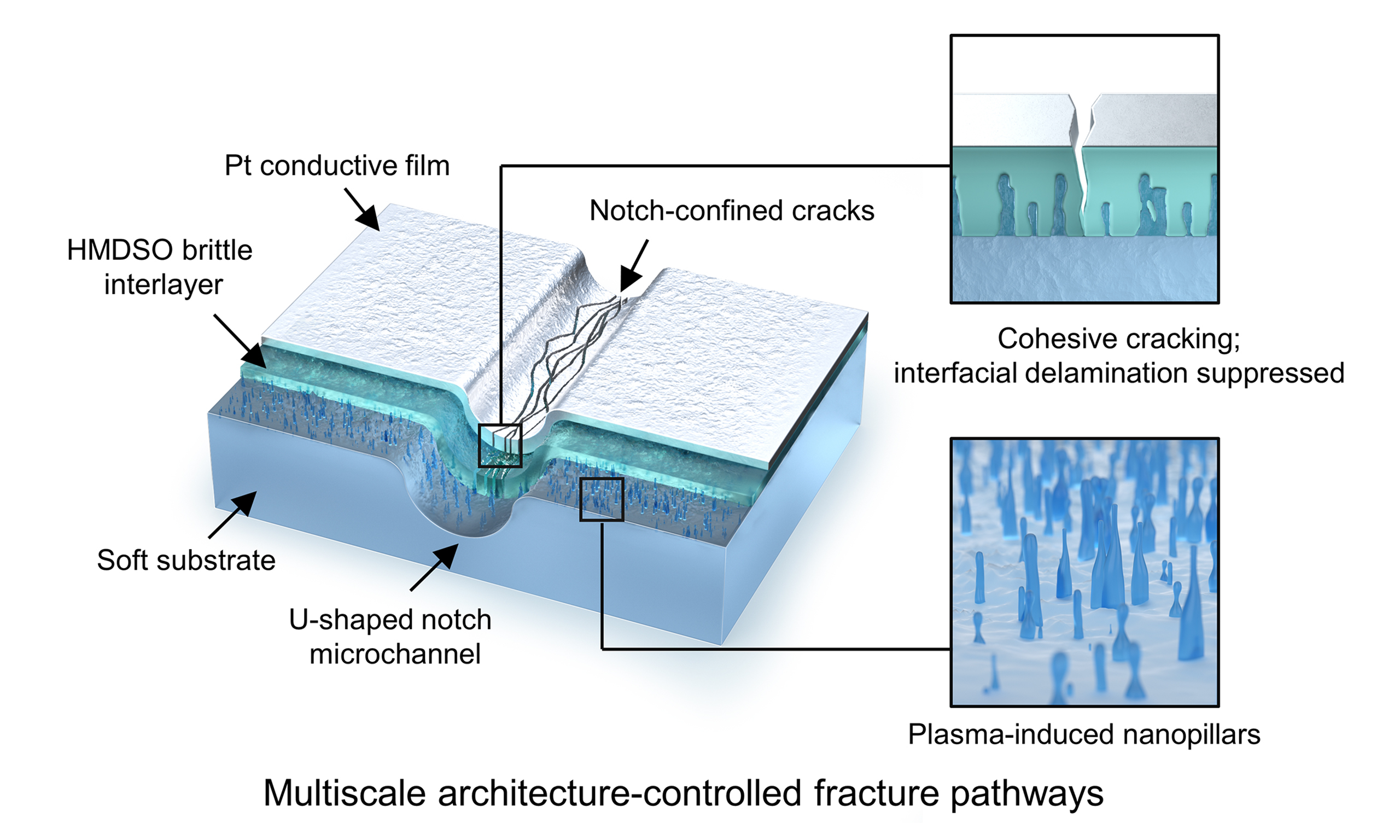
Cracks have been widely employed as functional elements in stretchable sensors exhibiting continuous resistance modulation under mechanical strain. Although the opening of an individual crack inherently induces a nonlinear, sharp increase in resistance, most strategies rely on dense multi-crack networks, in which statistical reconfiguration of percolation pathways averages the nonlinear behavior of individual cracks. Here, we present a strategy that transforms a multi-crack percolation system into a deterministic architecture with a small number of confined cracks, thereby enabling deterministic mechanical switching characterized by discrete on/off switching at a critical strain. To do this, a U-shaped notch microchannel and nanostructures are introduced on the top surface of soft substrates, which can prevent random crack initiation and suppress competing interfacial delamination of thin conducting films during repeated mechanical deformation of the substrate by taking advantage of mechanical interlocking-enhanced adhesion. This multiscale interface engineering selectively programs the dominant fracture pathway toward notch-confined crack opening and closing. The resulting device exhibits reproducible off-state and on-state switching during tensile loading and release, while maintaining stable baseline resistance over 210 cycles and showing low hysteresis. These results demonstrate that statistically governed dense crack-based devices can be redefined as deformation-driven mechanical switching, providing a fracture-pathway design principle for functional expansion of deformable electronics.
Keywords
INTRODUCTION
Deformable electronic devices - systems that endure and exploit mechanical deformation on compliant substrates - have developed strategies over the past decades through extrinsic structural design, thereby converting device deformation into electrical function[1,2]. For example, geometric approaches such as wrinkling[3], buckling[4], serpentine interconnects[5], and kirigami- and origami-based cuts[6,7] and folds[8] have become established in the field of deformable electronics as representative design paradigms that expand the intrinsic mechanical degrees of freedom of bulk materials[9,10], effectively redistributing local stress through geometric distortion, delaying fracture, and thus maintaining electrical continuity[11-14]. In parallel, micro- and nanoscale surface structuring has emerged as a key strategy for enabling extrinsic advantages in a wide range of wearable electronic devices[15-17]. Around the same period, crack-based electronic devices[18], featuring high gauge factors and simple processes, have emerged as an important technological axis in wearable electronics and biosignal monitoring[19]. From a physical perspective, unlike other geometric strategies that aim to maintain structural and electrical continuity, these crack-based approaches rely on a mechanism that explicitly exploits discontinuities in conductive pathways to program functionality. In the function, cracks intentionally formed under mechanical tension can open and close in response to substrate deformation, inducing the disconnection and reconnection of conductive pathways[20]. Such opening and closing of crack interfaces, in turn, dynamically create or remove conductive bottlenecks, respectively, thereby amplifying resistance changes in a nonlinear manner.
Significantly, in strategies employing multiple-crack networks for crack devices, the nonlinear response of individual cracks can be statistically averaged, yielding macroscopically quasi-linear behavior[21]. Such an averaged conductive pathway reconfiguration mechanism elevates crack architectures from structural, trivial defects to dynamic functional elements that regulate mechanoelectrical transduction. However, because this response relies on the statistical opening and closing of multiple-crack networks and the reconfiguration of percolation pathways, it inherently possesses structural limitations[22,23], including indeterminacy of conductive pathways, hysteresis, degraded cyclic stability, and device-to-device variation. Recognizing these limitations, research has expanded toward more precise control of crack networks, spanning the categories below: (1) crack-type engineering (e.g., metacracks[20] and fractal cracks[24]); (2) geometric parameter optimization[25] (e.g., asperity height, crack depth, and crack density) combined with finite element method (FEM)-based predictive modeling[26,27]; and (3) data-driven optimization incorporating AI-based strategies[28]. These developments have commonly been predicated on multiple-crack networks and have progressed toward optimizing percolation-based collective behavior through precise regulation of crack density and spatial arrangement.
In our recent study, we reported that even without a physical contact network in which numerous units mutually interfere, a small number of independent units alone can realize sufficient functional degrees of freedom and high information density[29]. Rather than employing randomly accumulating components and relying on statistical behavior, our strategy deterministically redefines system behavior by structurally constraining the operating range of a small number of spatially isolated units. From our perspective, this strategy can also be applied to crack devices currently based on multi-crack percolation, paving the way for an interesting approach that fundamentally reduces the number of cracks, thereby restricting conductive pathways to a small number of structurally defined bottlenecks. In this case, the conductive response is governed not by the statistical averaging of numerous cracks but by a few intentionally defined cracks, and the resistance change can be interpreted as a discrete transition characterized by a well-defined critical strain rather than probabilistic percolation in previous studies.
Here, we propose a strategy that transforms a multi-crack network into a deterministic small-number crack architecture by employing micro-nano structural interfaces. In our study, a metal layer on a soft substrate exhibiting distributed cracking behavior was defined as the reference system, and a micro-scale U-shaped notch was introduced to spatially confine crack initiation sites via programmable photopolymerization, thereby fixing the locations of conductive bottlenecks. Although stress concentration was amplified by creating U-shaped converging notches, additional cracks were generated outside the notched regions during tensile loading, which again exhibited multi-crack-network behavior. To resolve this, a hexamethyldisiloxane (HMDSO)/metal bilayer structure was introduced to guide cracks into specific regions; however, during cyclic tensile loading, a transition in fracture mode was observed, in which irreversible delamination (i.e., interfacial cracking) occurred at the opening interfaces instead of reversible crack opening (i.e., cohesive cracking). To address these issues in crack devices, we present a combined multiscale interface with a microscale U-shaped notch channel and nanoscale pillar structures, which can enhance substrate/HMDSO interfacial adhesion and structurally suppress delamination over cyclic tests. As a result, the dominant fracture pathway was programmed to be notch-confined crack opening, thereby enabling a stable crack architecture in which only a small number of structurally defined cracks determine the conductive state. Our structure exhibited low hysteresis and improved cycling stability, and displayed discrete transition behavior at a well-defined critical strain. Significantly, the conductive response is not continuously modulated by probabilistic percolation but is selectively switched off and on by the opening and closing of structurally defined cracks. This mechanism demonstrates that only a few crack-based elements can be exploited as deterministic mechanical switching that deterministically control conductive channels in response to mechanical input in deformable electronics.
EXPERIMENTAL
Fabrication of soft substrates with U-shaped micronotches
An ultraviolet (UV)-curable resin (NOA 73, Norland Products) was used for the fabrication of deformable substrates. The resin was coated to a uniform thickness of approximately 100 µm, which was defined as the reference thickness to ensure a stable z-directional distribution of UV intensity and reproducible notch–bridging formation depth. UV patterning was performed using our recently reported digital micromirror device (DMD)-based maskless projection system[30]. To generate U-shaped notches, the exposure dose was adjusted to induce partial curing in regions exceeding the depth of focus (DOF) while maintaining in-plane pattern resolution. For this purpose, the upper bound of UV energy required to preserve the planar resolution of the curing pattern was predetermined, and exposure conditions were found within this range. The UV intensity was set to 409 mW/cm2, and the exposure time was fixed at 0.6 s, resulting in a total exposure dose (dose = I × t) of 245.4 mJ/cm2. These conditions were identified within a process window where upper gap retention and lower bridging formation were simultaneously achieved [Supplementary Video 1]. After exposure, uncured resin inside the notch region was removed by mild acetone immersion for 10 s at room temperature, followed by a fresh ethanol rinse to eliminate residual uncured resin. A subsequent UV post-curing step was then performed for 60 min to ensure complete curing and structural stabilization of the surrounding matrix.
Plasma treatment for nanostructuring
Plasma treatment was performed to enhance polymer–HMDSO interfacial adhesion. The purpose of the treatment was to form nanoscale surface structures on the soft substrate[31], thereby increasing the effective contact area with the HMDSO layer later. In particular, under the condition without nanostructuring (i.e., Cond. 3), interfacial delamination at the HMDSO layer was observed during cyclic tensile loading. To address this issue, a plasma-induced nanostructuring (i.e., Cond. 4) was introduced. Plasma treatment induced modifications in surface topography as well as surface properties (mechanical strength, hardness, and surface energy), which can alter the stress-mismatch conditions at the interface with the HMDSO layer. Excessive stress mismatch may lead to wrinkle formation; therefore, process optimization is required. The plasma treatment time was set to 200 s as the baseline condition, and additional conditions of 100 and 300 s were evaluated for comparison. The process was conducted under O2 RF glow-discharge plasma conditions (20 mTorr, 50 W and 20 sccm).
HMDSO and Pt deposition
HMDSO was employed as a brittle interlayer to induce crack formation. The HMDSO thin film was deposited using plasma-enhanced chemical vapor deposition (PE-CVD) with a thickness of 120 nm. The thickness of the HMDSO layer is a parameter influencing crack-initiation stability and interfacial stress conditions. Pt was used as a conductive electrode layer for electrically measuring the open/close behavior associated with crack formation. The Pt thin film was deposited by vertical sputtering. The thickness of the Pt layer was 30 nm. The thickness was determined by balancing electrical continuity and crack sensitivity. When the Pt layer is thin, the initial resistance increases, but the sensitivity to crack formation is enhanced, leading to more pronounced switching behavior. Conversely, increasing the thickness generally improves electrode continuity; however, resistance variation tends to become more gradual, which may weaken abrupt switching behavior depending on the fracture mode.
Tensile testing setup
A precision linear-stage-based tensile system was configured for simultaneous electromechanical measurements. The specimens were clamped at both electrode pads to ensure load transfer along the tensile direction, and the initial gauge length (L0) was set to 1.5 mm. Two tensile modes were employed. First, the monotonic tensile test involved continuous tensile loading at a constant speed to evaluate the behavior up to mechanical fracture or electrical disconnection. Second, the cyclic tensile test was used to assess cyclic stability and hysteresis by stretching the specimen to a target strain, then repeating loading–unloading cycles. The tensile speed was set to 0.01-1 mm/s and carefully adjusted depending on the measurement objective. The applied strain range was 10%-100%, and tests were conducted using stepwise increases in strain to evaluate the structure’s mechanical stability and conductive transition behavior.
Electrical measurement
Electrical resistance was measured using a two-point probe configuration. The devices fabricated in this study exhibited initial resistances on the order of several kΩ, which increased to several MΩ upon crack opening. Therefore, the two-point measurement method was considered sufficient in terms of measurement accuracy. Because the two-point configuration can be sensitive to contact resistance and variations in clamp conditions, the contact pressure between the electrode pads and the clamps was standardized to maintain consistent contact conditions. In the tests, screw-type clamps were used, and the same applied torque condition of 0.200 ± 0.001 Nm was consistently applied to all devices. Prior to the main measurements, all specimens were subjected to an initial preconditioning cycle until the baseline resistance stabilized at approximately 3 kΩ. This procedure was introduced to eliminate the initial microcrack stabilization regime and to standardize all specimens under the same baseline condition before comparative measurements. All electrical responses are reported as normalized resistance ratios (R/R0), where R0 denotes the baseline resistance measured after preconditioning. This normalization ensures that device-to-device variations in absolute initial resistance, which may arise from the intentionally high sputtering pressure (~55 mTorr) used during Pt deposition, do not affect the comparative interpretation of crack-opening behavior and switching reproducibility.
Data acquisition and signal processing
Resistance data were logged in real time in synchronization with tensile deformation. The data acquisition software included a median-filter–based noise-reduction function for signal stabilization, and a cutoff filter option was applied when necessary. The determination of the open state (conductive disconnection) was performed based on a predefined resistance threshold. The strain at the crack-open state, εopen, was defined as the strain at which the resistance exceeded the specified cutoff value. In this study, R ≥ 10 MΩ was adopted as the criterion for the crack-open state. This threshold was determined considering the upper measurement limit of the instrumentation and the background noise level.
Image processing and analysis
Scanning electron microscopy (SEM) images were analyzed using the ImageJ Ridge Detection plugin (σ = 1.94, lower threshold = 1.70, upper threshold = 4.59, line width = 9) to quantify crack length, width, and orientation. Crack segments shorter than 100 nm were excluded, as they cannot be reliably distinguished from surface contrast noise at the SEM resolution used in this study.
RESULTS AND DISCUSSION
From distributed crack networks to pathway-controlled few-crack architecture
The schematic illustrations in Figure 1 describe the transition from multi-crack-network-based behavior to mechanical switching based on a small-number-crack architecture, in which the fracture pathway is selectively and locally controlled. In the reference structure (i.e., Cond. 1 in Figure 1A), where a thin Pt layer is deposited on a planar NOA substrate, numerous cracks form in a spatially distributed manner as the tensile load increases (here, unidirectional loading). The cracks primarily align perpendicular to the direction of tension, although randomly generated cracks also coexist and exhibit an overall statistical distribution [Supplementary Figure 1]. As a result, the network formed by these multiple cracks alters the conductive pathways, and the electrical response is determined by collective percolation behavior. The strain-resistance curve exhibits a macroscopically continuous and averaged increase, while the opening and closing behavior of individual cracks is integrated into the overall network response.
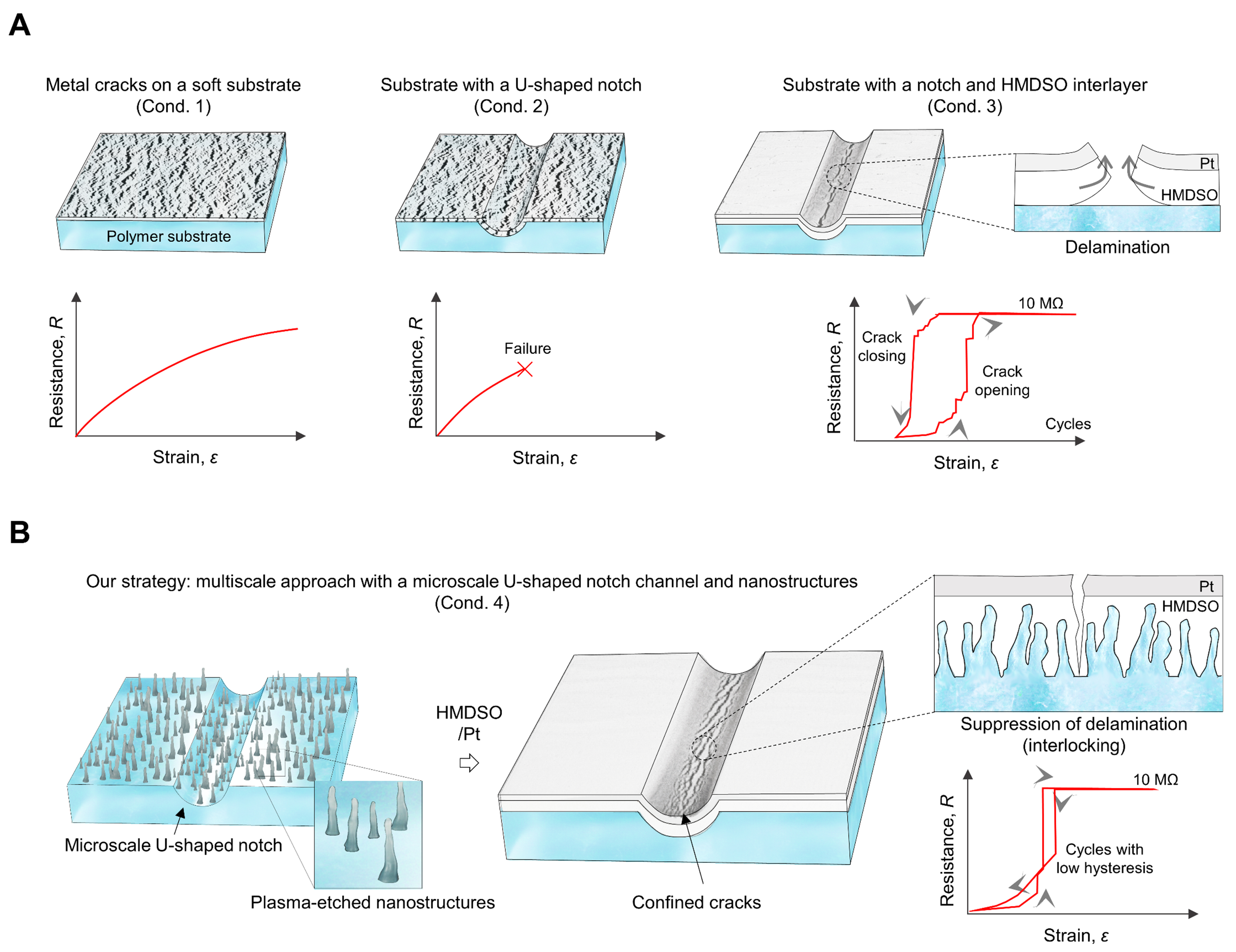
Figure 1. From distributed crack sensors to confined cracks for mechanical switching. (A) Three crack-device configurations. Cond. 1: a metal crack layer formed on a flexible flat substrate. Cond. 2: a metal crack layer formed on a U-shaped notch. Cond. 3: a metal crack layer formed on a flexible notched substrate incorporating a brittle interlayer (HMDSO). Cond. 1 and Cond. 2 exhibit conventional crack-based resistive sensing behavior as a function of applied strain. In contrast, Cond. 3 shows an abrupt resistance increase (up to ~10 MΩ) due to crack opening prior to substrate fracture; however, cyclic reliability is limited due to interfacial delamination; (B) Micro–nano structural strategy for fracture pathway control. Cond. 4: A confined metal crack layer on a microscale U-shaped notch combined with plasma-induced surface nanostructuring suppresses interfacial delamination of the HMDSO/metal films and enables stable crack opening and closing, thereby establishing mechanical switching behavior. HMDSO: Hexamethyldisiloxane.
To spatially confine crack initiation through stress concentration, a microscale U-shaped notch was introduced into the substrate on which a metal crack layer was formed (i.e., Cond. 2). This geometry was selected because its stress concentration factor is relatively lower than that of a V-shaped notch, providing more favorable conditions for fracture-mode control. In this structure, cracks in the metal layer were confirmed to initiate preferentially near the notch; however, as tensile strain increased, additional cracks emerged in regions outside the notched area. This indicates that while the notch can induce crack initiation, it cannot fully control crack propagation or subsequent crack-generation pathways. Consequently, the conductive response continued to exhibit multi-crack network behavior, and complete crack localization was not achieved.
To further concentrate crack formation within the notched region, an HMDSO-based brittle interlayer was introduced above the entire surface of the notched substrate (Cond. 3: notched substrate/HMDSO/Pt layer). This modification was intended to reorganize the stress distribution and guide cracks toward a specific location. However, during cyclic tensile loading, a fracture-mode transition was observed, with interfacial delamination at the HMDSO-soft substrate interface becoming dominant. The strain-resistance response exhibited irreversible increase and hysteresis, indicating that the crack-localization strategy activated a new interfacial fracture pathway. These results suggest that the phenomena lie not merely in stress concentration, but in how the energetic priority among competing fracture pathways is redistributed.
Accordingly, the central proposition found in these demonstrations is as follows: merely introducing a micro-scale U-shaped notch is insufficient to control crack localization, and the energetic competition between cohesive cracking in the metal film layer during crack opening and delamination under interfacial crack modes (i.e., Mode I vs. II) must be redesigned to guide the dominant fracture pathway selectively. To address this issue, as shown in Figure 1B, we introduced micro-nano interfacial structuring (Cond. 4). Nanoscale surface roughness was generated on the surface of the soft polymeric substrate via plasma treatment[31], thereby increasing the interfacial contact area with the HMDSO layer and enhancing mechanical interlocking. Within such structures, the critical energy for interfacial fracture increases, thereby suppressing the delamination pathway (i.e., interfacial crack propagation) in our current crack device in a similar manner. The fracture pathway of the metal layer is reselected to the notch-confined crack-opening mode, and cracks localize to a small number of structurally defined positions. Consequently, the conductive state is governed by a few cracks, and the resistance response exhibits a discrete transition with low hysteresis at a well-defined critical strain. Overall, Figure 1 conceptually summarizes the transition from the statistical percolation behavior of multi-crack networks to a strategy that selectively programs the dominant fracture pathway by structurally redesigning the competition between interfacial energy and fracture pathways. This approach does not merely reduce the number of cracks; rather, it reconstructs the energetic landscape of competing fracture modes to deterministically define conductive pathways, thereby establishing the foundation for crack-confined switching in which deformation operates not as continuous resistance modulation but as selective switching of conductive states.
DOF-engineered notch fabrication via off-focus slit convergence
Figure 2 presents the design mechanism of U-shaped microscale notches to confine crack initiation in our strategy. In this study, we demonstrate a photocuring-based manipulation of notches using our light-writing setup[30], here applying a proximity effect that transforms the optical DOF into an active design parameter. The DOF of an optical system is determined by the numerical aperture (NA) of the lens and the operating wavelength (λ), and can generally be approximated as[32]
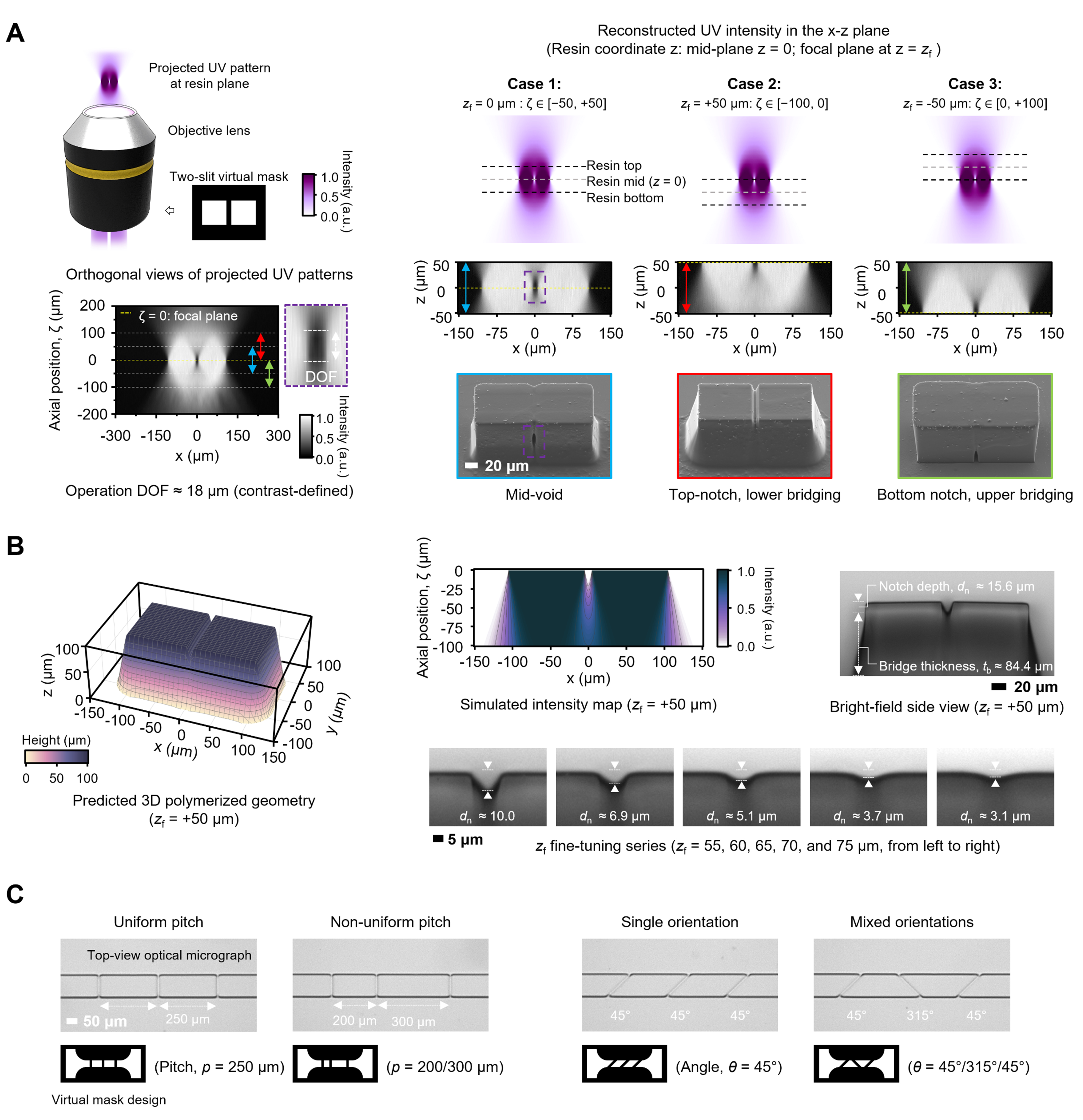
Figure 2. Fabrication of a U-shaped notched substrate using a photocurable material. (A) Orthogonal view of the projected UV intensity distribution with respect to the position of the sample focal plane (zf). The inset shows experimentally measured light intensity profiles. Using a 20× objective lens, a DOF of approximately 18 μm is observed in the x-z plane. Case 1-3 illustrate representative photocured structures obtained at different zf positions, resulting in a central void, a top-surface notch, or a bottom-surface notch, respectively; (B) Comparison between simulated photocured structure profiles and experimental results. The inset shows the notch depth generated at different zf values; (C) Programs for controlling the periodicity and notch angle. UV: Ultraviolet; DOF: depth of focus.
representing the effective z-directional range around the focal plane within which the pattern geometry is maintained. In general, as NA increases, the DOF decreases. When the working plane of the specimen is positioned within the DOF range, as illustrated in Figure 2A, the two slit patterns in the virtual mask are optically reproduced as separated features (see the yellow line in the orthogonal view of the projected UV patterns), which in turn forms a void region at the focal plane with a sample having sufficiently large height (here, the thickness of UV resin film ~100 μm). Our experimental visualization shows that, as in Case 1 (i.e., for focal plane at zf =0 μm) in the figure, a discontinuous region of approximately 18 μm along the z-direction is observed inside the polymerized structure in the SEM image, which corresponds to the DOF ~18 μm in the orthogonal views of the projected UV patterns. Under this condition of zf =0 μm, the light intensity distribution remains most confined near the focal plane, and light intrusion into the gap region between the slits is minimized, thereby maintaining structural separation along the depth direction.
In contrast to this conventional operation, as illustrated in Cases 2 and 3, we intentionally introduced a defocus offset (Δz) along the z-axis of the specimen and used the change in the light-intensity distribution under conditions beyond the DOF range as a design variable. Specifically, when the specimen is displaced from the focal plane either upward (+Δz) or downward (-Δz), the projected UV pattern spreads along the z-direction due to diffraction and geometric divergence, and the optical field around the slits gradually expands in depth. As a result, the light intensity distribution near the gap region between the slits evolves from the previously separated state at a single plane and tends to overlap along the depth direction. In particular, under conditions with a non-zero Δz, overlap of the optical field occurs asymmetrically along the depth direction. When the specimen is positioned above the focal plane, converging rays first overlap in the upper region, forming a U-shaped structure connected to the bottom (Case 2). Conversely, when the specimen is positioned below the focal plane, diverging rays overlap in the lower region, resulting in an inverted U-shaped structure connected from the top (Case 3).
In optics, this slit convergence phenomenon is governed by the NA, λ, and Δz, and can be quantitatively described using a Fresnel diffraction-based optical propagation model (see the simulation and measurement results in Supplementary Figure 2). Figure 2B directly correlates the predicted DOF-based notch formation mechanism with experimental observations. Optical propagation simulations were performed to calculate the Δz-dependent redistribution of light intensity, from which the location and geometry of slit overlap were quantitatively predicted. For photopolymerization simulation, defocus-induced blurring was approximated using Gaussian convolution, with the blur width determined by the combined diffraction and geometric divergence components. This analysis visualizes the progressive lower-region overlap and gap invasion in the x-z plane [Supplementary Figure 3], confirming that bridging formation is a deterministic optical consequence of Δz rather than a process fluctuation. In such a strategy, the resin thickness is a critical process parameter. Under the 100 μm thickness condition, the position at which the upper gap is preserved and the depth at which bridging forms are determined by the z-directional attenuation and diffusion of light [Supplementary Figure 4]. As the thickness increases, absorption and scattering effects may shift the overlap region, potentially affecting the effective notch depth and the position of the stress concentration. The slit gap itself is also highly geometry-sensitive. When the gap is reduced to 5-7 μm, optical overlap occurs more readily, potentially decreasing the notch depth. Conversely, when the gap is increased to 12-15 μm, insufficient lower bridging may occur, weakening structural connectivity. The 10 μm gap selected in this study was identified as a balanced condition that maintains the upper separation while enabling stable lower bridging formation.
Through this parametric design study, Figure 2C presents the results obtained by systematically varying the spacing between notches, and array angle within the virtual mask. Modulating the slit linewidth adjusts the width of the convergence region and the notch opening width, while the slit spacing determines the notch depth and the critical Δz window for structural connection. In addition, tuning the slit array angle enables control over the notch opening angle and the direction of stress concentration. These results demonstrate that the notch geometry is not fixed as a single configuration but is continuously tunable within an optical parameter space. Accordingly, the notch width, depth, and opening angle can be defined as independent or coupled design variables, representing a transition from simply inserting defects to engineering the fracture initiation geometry itself. In this study, the notch geometry was selected as a representative working geometry that balances notch-confined crack opening and conductive continuity, rather than as a fully optimized configuration across all geometric parameters. Within a practical notch-depth working regime, the switching response was preserved during repeated cycling even for specimens with intentionally deeper notches [Supplementary Figure 5]. A comprehensive optimization coupling notch width, depth, and opening angle with fracture-mechanics analysis remains an important direction for future work. Whereas conventional notch fabrication methods rely on mechanical milling[33], laser processing[34], or etching[35] to form shapes in post-fabrication, the present approach actively employs optical DOF and energy distribution as design parameters to define structure formation.
Electrical response and fracture-mode competition in notch-engineered crack systems
As shown in Figure 3, a Pt film was deposited onto the previous structures (i.e., Cond. 1-3), and the electrical response under tensile loading was monitored in real time. To precisely validate the crack-based behavior, an automated electromechanical measurement system was constructed using a motorized linear stage [Figure 3A], enabling high-precision synchronization of tensile strain and resistance variation. Considering the possibility that the conductive pathway may be significantly altered, the measurement setup was configured to sensitively analyze the correlation between crack-initiation events and resistance changes, specifically those expected in the tests with samples in Cond. 3. The SEM image in Figure 3B shows the top surface of the sample in Cond. 3, where the crack is monitored in the U-shaped notch area, while some aligned crack lines are also shown along the tensile loading direction.
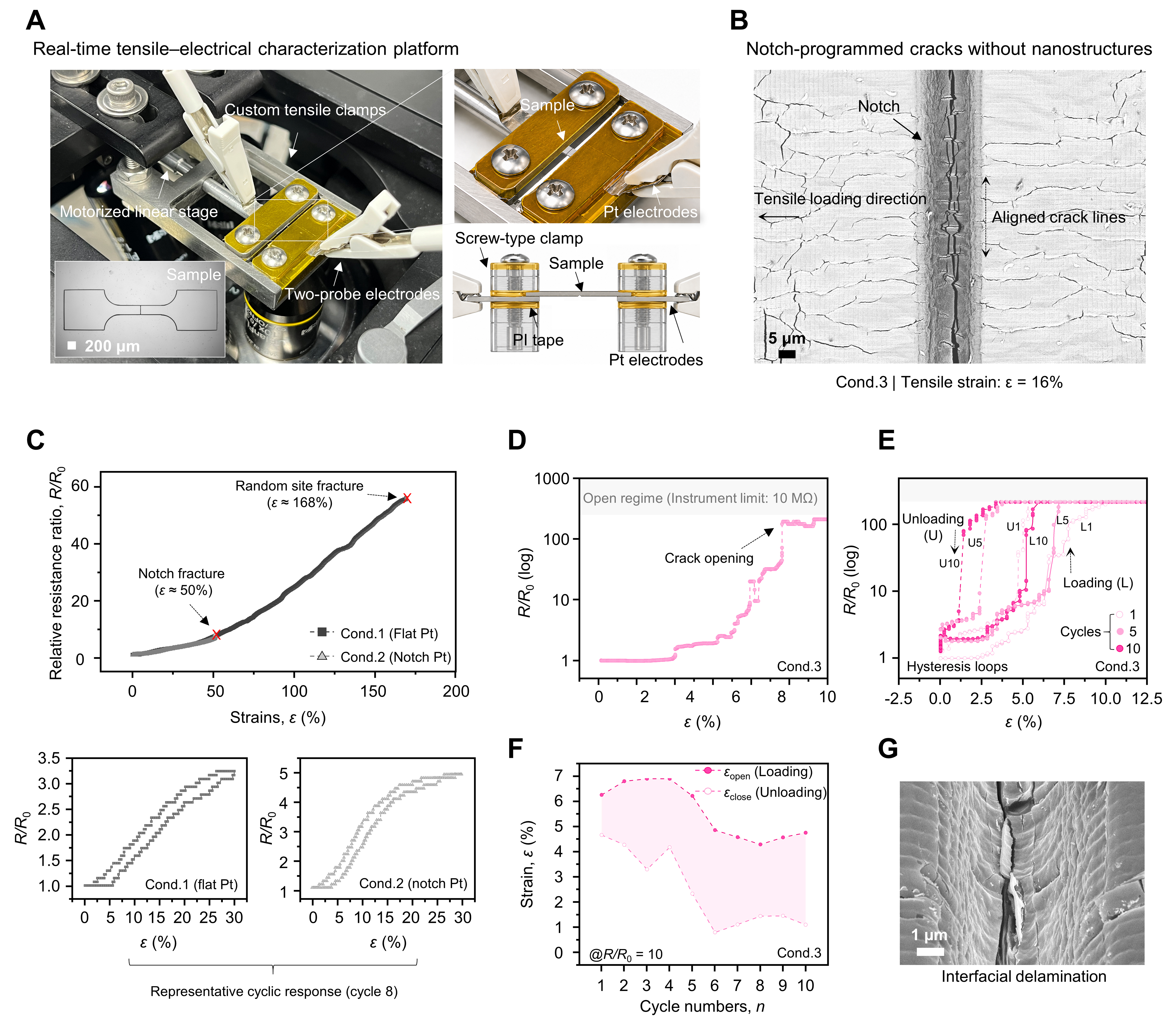
Figure 3. Electrical characterization of crack-based devices. (A) Schematic illustration of the electromechanical characterization platform for simultaneous tensile and electrical measurements of U-shaped notch specimens under uniaxial loading. (Right) Top-view enlarged image of the sample fixation region (top) and cross-sectional schematic of the clamp configuration (bottom). The schematic depicts the polyimide double-sided adhesive layer between the specimen and the clamps, the two-point measurement configuration contacting the Pt electrode pads, and the screw-type clamping that maintains uniform contact pressure across all specimens. The active sensing region is rectangular (200 µm × 1.5 mm), with the U-shaped notch positioned at its geometric center; (B) SEM image of a Cond. 3 device at ~16% strain. The notch structure and crack formation are observed, with multiple cracks on the surface. These stripe-like features are not cracks but buckling-driven delamination morphologies; (C) Electrical response of Cond. 1 and Cond. 2 devices. The resistance increases gradually with applied strain, similar to conventional crack-based resistive sensors. The notched sample showed an earlier mechanical fracture; (D) Electrical response of the Cond. 3 device. A sharp resistance increase (up to ~10 MΩ) occurs at ~8% strain, corresponding to a crack-opening behavior prior to substrate fracture; (E) Cyclic tensile test of the Cond. 3 device, showing a mismatch between the strain at crack opening (εopen) and closing (εclose); (F) Evolution of εopen and εclose, characterized at R/R0 = 10 over 10 cycles. The values fluctuate and do not converge from cycle to cycle; (G) SEM image showing interfacial delamination of the HMDSO and metal films from the polymer substrate. SEM: Scanning electron microscopy; HMDSO: hexamethyldisiloxane.
The electrical characteristics of the reference structure (i.e., Cond. 1), in which Pt was deposited on a planar substrate, were first evaluated as presented in Figure 3C. As tensile strain increased, randomly distributed multiple cracks formed at multiple locations, and the resistance increased continuously with increasing strain. The initial resistance was approximately 1.1 kΩ, and physical fracture of the sample occurred at a strain of ε ~ 168%. Prior to fracture, the relative resistance ratio (R/R0, where R0 is the initial resistance of the sample) reached approximately 55, representing a typical sensor-type response characterized by continuous resistance variation over a wide strain range. In the structure with a microscale U-shaped notch (i.e., Cond. 2), the resistance response to mechanical deformation initially exhibited a trend similar to that of Cond. 1. Due to the presence of the notch, fracture occurred rapidly at ε ~ 50%, and R/R0 increased with a nearly constant slope until fracture. In the cyclic tests for both samples (Cond. 1 and 2) in a small strain regime (ε < 30%), the resistance changes followed a linear and averaged response, and no discrete on-off transition in electrical signals was observed (see the lower two plots in Figure 3C).
It should be noted that in the sample incorporating an HMDSO layer at the notch (i.e., Cond. 3), electrical switching was observed prior to mechanical fracture during tensile loading, as a few cracks opened. As shown in Figure 3D, the resistance sharply increased at approximately ε ~ 8%, resulting in a loss of conductivity. This suggests that the notch-confined crack can enable tension-induced switching behavior. However, unfortunately, under repeated loading-unloading cycles, this device exhibited pronounced hysteresis loops and cycle-to-cycle drift, as shown by the 1st, 5th, and 10th loading–unloading cycles of the same device (L1, L5, L10 in Figure 3E). Notably, εopen progressively shifts toward higher strain values with increasing cycle number, directly demonstrating that the switching strain in Cond. 3 is not stably maintained but instead drifts cycle-to-cycle. In particular, both discrepancies between εopen and εclose, defined at a specific resistance ratio of R/R0 = 10 for crack opening and closing during loading and unloading, respectively, and cycle-dependent variations, were observed [Figure 3F]. These results indicate that under repeated loading, although the substrate notch enables early crack opening along the notch direction, the crack-opening mode does not remain energetically dominant; instead, a competitive transition to interfacial delamination occurs [Figure 3G], ultimately leading to failure under cyclic operation. This result demonstrates that geometric stress concentration alone is insufficient to secure deterministic behavior based on a small number of cracks. Notably, a competitive relationship exists between crack opening within the thin film and interfacial delamination, and when interfacial adhesion strength is not sufficiently secured, delamination can be selected as the dominant fracture mode[36,37]. Once a crack propagating within the film reaches the film-substrate interface, if the interfacial adhesion strength is low, the crack deflects and propagates along the interface, thereby causing delamination. In general, as an interfacial crack advances, the in-plane shear-dominated fracture component (Mode II) increases, promoting delamination along the interface. Furthermore, when the substrate surface is not perfectly flat and contains undulations or defects, increasing strain can activate the out-of-plane fracture component (Mode I). The enhancement of Mode I-driven interfacial crack opening further accelerates interfacial delamination and becomes a major contributing factor to its progression. Therefore, the stable implementation of few-crack-based deterministic switching requires not only a precise definition of the crack initiation geometry but also a structural redesign of the energetic hierarchy among the competing fracture pathways.
Reversible crack-based mechanical switching via multiscale fracture pathway control
We experimentally demonstrate that a multiscale strategy, i.e., combining microscale U-shaped notch-based geometric control with nanoscale interfacial structuring, can transform a crack-based device into a reversible mechanical switching architecture by redesigning the energetic hierarchy of competing fracture pathways as presented in Figure 4. To do this, nanoscale surface roughness was introduced onto the polymer substrate via plasma treatment, as illustrated in Figure 4A. First, nanoscale structures formed perpendicular to the interface, originating from the plasma-etched substrate, increase the effective interfacial area between the film and the substrate, thereby enhancing interfacial adhesion. In addition, even if a film crack partially transitions into an interfacial crack, its propagation along the interface is suppressed by the nanoscale structures. This effect arises because the out-of-plane fracture component (Mode I) of the interfacial crack is effectively constrained, thereby hindering crack propagation.
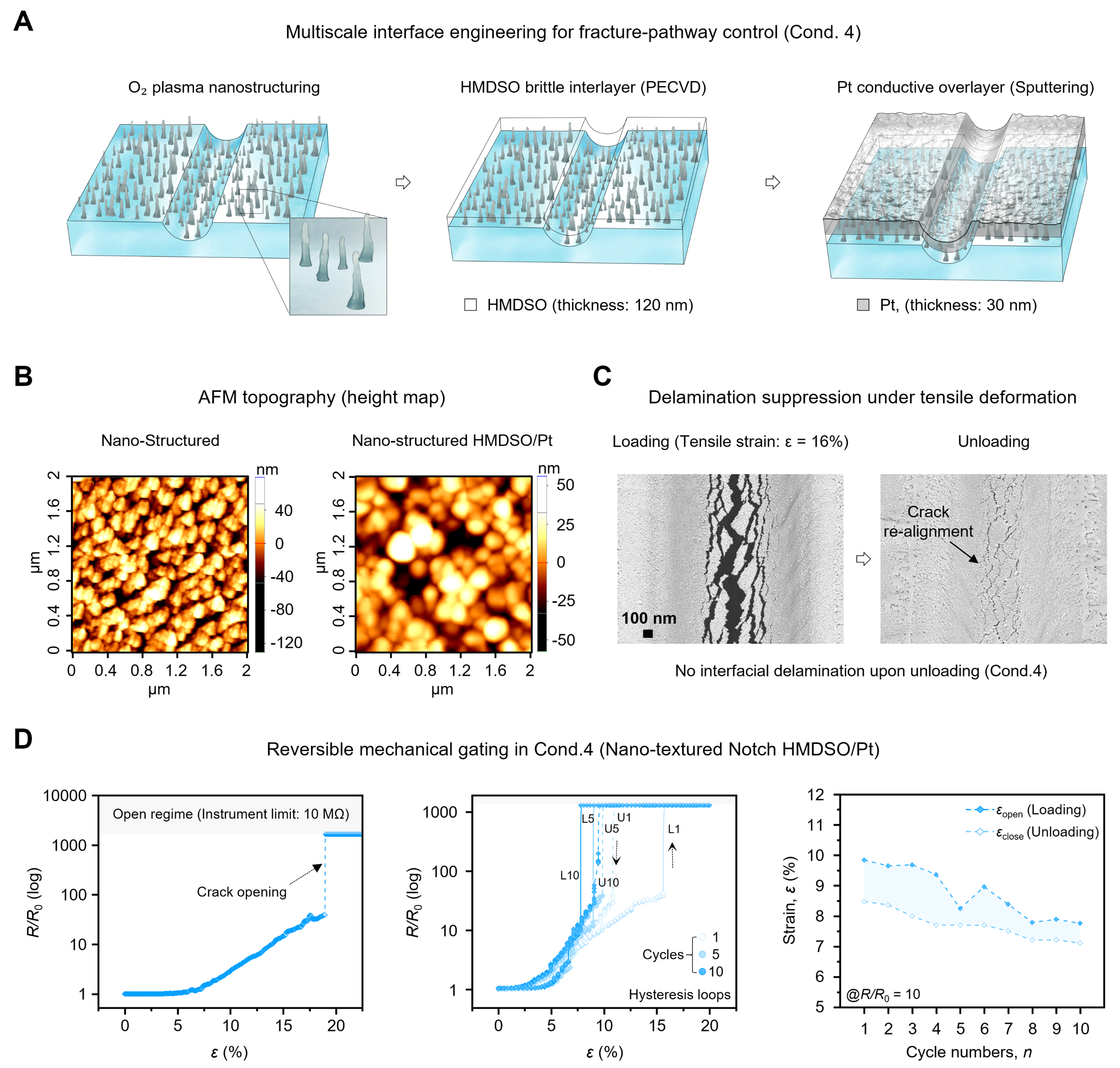
Figure 4. Fracture-pathway control through multiscale interface engineering. (A) Schematic illustration of the fabrication process. Oxygen plasma treatment generates nanoscale structures on the etched polymer surface. Subsequent deposition of HMDSO forms strong interfacial adhesion through mechanical interlocking; (B) AFM images. (Left) Nanoscale surface structures formed after plasma etching. (Right) Surface morphology after HMDSO/Pt deposition; (C) SEM images at 16% tensile strain and after strain release. Crack formation is suppressed on the planar region outside the notch, and film delamination at the notch is significantly reduced. Upon unloading, structural conformity between the separated crack faces is maintained; (D) Electrical characterization results. (Left) Under monotonic tensile loading, the crack opens at ~18% strain. (Middle) Cyclic tensile test over 10 cycles, showing convergence of εopen and εclose with increasing cycle number. (Right) Evolution of εopen and εclose, defined at R/R0 = 10. The average Δε (= εopen - εclose) over 10 cycles is 1.06% ± 0.44%, indicating a small strain hysteresis. HMDSO: Hexamethyldisiloxane; AFM: atomic force microscopy; SEM: scanning electron microscopy; PECVD: plasma-enhanced chemical vapor deposition.
Atomic force microscopy (AFM) analysis in Figure 4B confirms the formation of nanoscale structures on the soft substrate after plasma treatment, and the increase in root-mean-square (RMS) roughness, together with changes in interfacial contact characteristics, support an increase in the critical condition for interfacial fracture. While this roughness increase is beneficial for interfacial adhesion, it is important to note that, although the RMS roughness increased to approximately 24.2 nm immediately after plasma treatment, subsequent deposition of 120 nm HMDSO and 30 nm Pt reduced the surface RMS roughness to approximately 16.6 nm, as the deposited films conformally follow the envelope of the underlying nanostructures [Supplementary Figure 6]. Accordingly, the elevated initial R0 observed in this study is more directly attributable to the intentionally high sputtering pressure (~55 mTorr) used during Pt deposition, which promotes a more porous-like microstructure and higher sheet resistance, rather than to surface-roughness-induced disruption of the percolation network. Multi-device statistics further support that this elevated resistance level is a reproducible feature of the selected deposition condition. The Notched Cond. 4 specimens exhibited an initial resistance of 3.68 ± 1.73 kΩ (n = 7) prior to preconditioning, whereas the Notch-free Cond. 4 control fabricated by the same process exhibited 2.53 ± 0.47 kΩ (n = 5), both within the same kΩ range [Supplementary Figure 7]. The larger variability of the Notched Cond. 4 is consistent with the localized geometric bottleneck introduced by the notch, rather than with instability of the Pt deposition process. These structural modifications reconstruct the fracture energy landscape, suppressing the delamination pathway and maintaining notch-confined crack opening as the energetically dominant mode. To verify this mechanism, as shown in Figure 4C, the sample, fixed on a tensile jig, was deformed and then placed in the SEM to observe cracks confined to the notch area. As the strain increased, cracks initiated and opened in a limited number along the notch direction, and no interfacial delamination was observed upon load removal. Moreover, upon reclosure, the opposing crack faces exhibited good morphological conformity with well-matched crack interface contact. This indicates that the multiscale interfacial design stabilizes the crack-opening mode as a reproducible pathway under cycling operation [Supplementary Figure 8]. Collectively, these results clarify the respective roles of the three key structural components: (i) the U-shaped notch acts as a geometric stress concentrator that defines crack initiation locations; (ii) the brittle HMDSO interlayer induces a cohesive fracture pathway for crack-mediated conductive transition; and (iii) the plasma-induced nanostructure suppresses interfacial delamination and provides cyclic interfacial stability [Supplementary Figure 9].
The electrical characteristics also clearly reflect this behavior. Under monotonic tensile loading, the resistance of a representative Cond. 4 device sharply increased and reached the open-state threshold
Reproducible mechanical switching with cyclic stability
To further examine the rapid stabilization behavior observed in the early cycles (εopen ≈ εclose) under long-term operation, cyclic tensile–release tests up to 210 cycles were performed on both Cond. 3 and Cond. 4 samples, as shown in Figure 5. The experiments were conducted under three distinct regimes with different loading speeds, and the base resistance ratio was tracked for each cycle, defined as Ri/R0, where Ri is the resistance at the crack-closed-state of each cycle [Figure 5A]. The 210 cycles were divided into three regimes as follows: Regime 1: tensile speed v ≈ 0.1 mm/s, displacement = 0.2 mm; Regime 2: v = 0.5 mm/s, displacement =
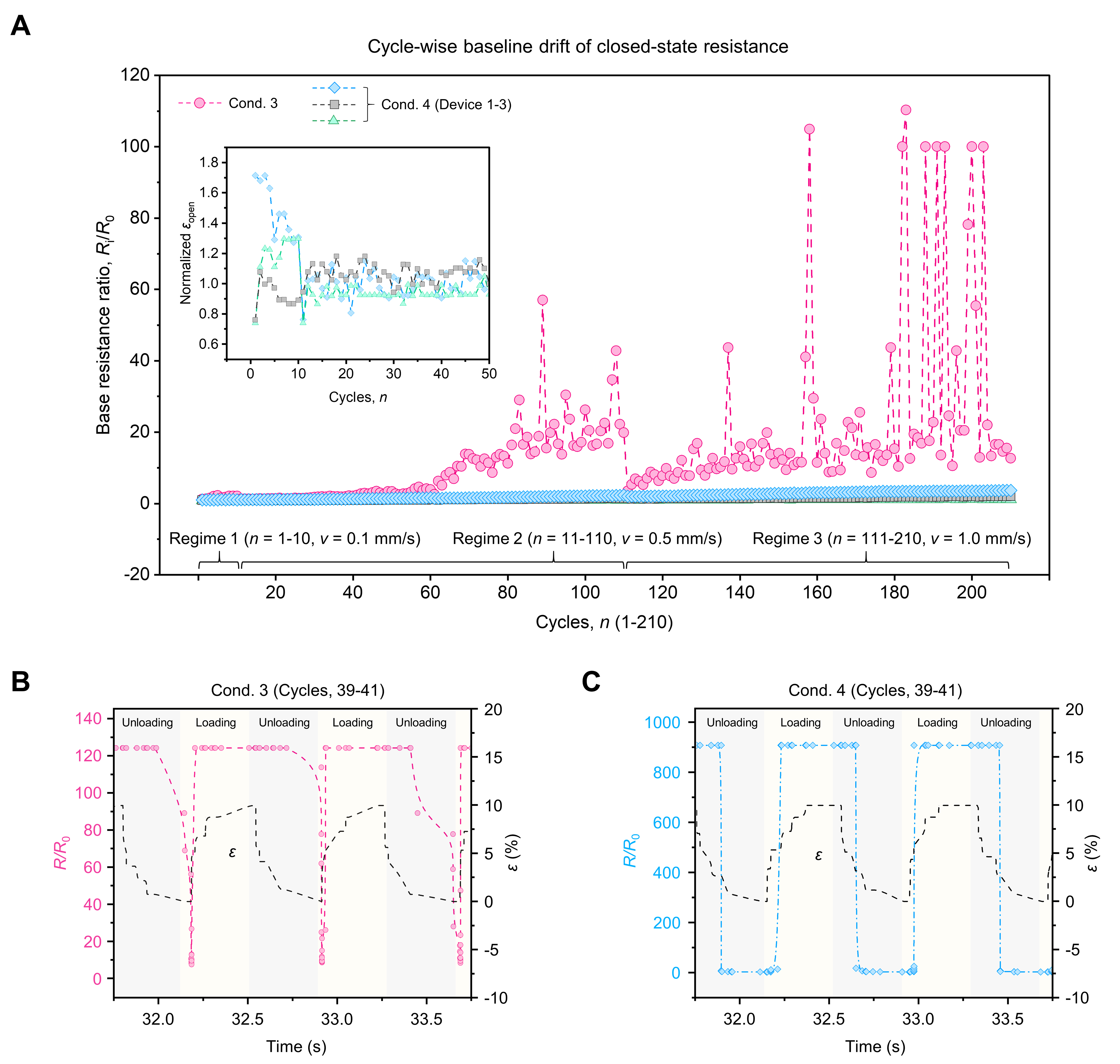
Figure 5. Cyclic stability of crack-based mechanical switching. (A) Cycle-by-cycle baseline R/R0 of Cond. 3 and Cond. 4 over 210 cycles under three tensile speed conditions (0.1, 0.5, and 1.0 mm/s). Three independent Cond. 4 devices are shown overlaid (Device 1: range 0.84-1.24, mean 1.04; Device 2: range 0.80-2.01, mean 1.33; Device 3: range 1.01-3.70, mean 2.19), in clear contrast to the long-term cyclic drift of a single Cond. 3 device (mean R/R0 ≈ 15.5, maximum up to ~110). Inset shows the normalized switching strain (εopen/‹εopen›steady) as a function of cycle number for the same three Cond. 4 devices, demonstrating convergence to unity within the initial ~10 cycles and stable maintenance thereafter; (B) Resistance–time curves of the Cond. 3 sample during cyclic loading and unloading. Although loading and unloading occur over identical time intervals, resistance recovery is delayed. This delay is attributed to contact re-formation kinetics of the delaminated film rather than mechanical recovery of the substrate; (C) Resistance–time curves of the Cond. 4 sample during cyclic loading and unloading. The device exhibits rapid and synchronized on-state and off-state switching in response to mechanical deformation.
Figure 5B and C present representative tensile–release responses for Cond. 3 and Cond. 4, respectively. The black dashed lines represent the applied mechanical strain profile, while the lines with circular markers correspond to the measured resistance response. The Cond. 4 device exhibits rapid and synchronous electrical tracking of the cyclic substrate deformation, and the opening and closing of the crack are consistently reproduced across cycles. These results demonstrate that the proposed multiscale fracture pathway control strategy stabilizes crack opening as the energetically dominant mode, thereby enabling reliable mechanical switching under repeated loading. Accordingly, the threshold-like switching behavior, hysteresis suppression, and baseline stability observed in Cond. 4 are not merely electrical performance metrics, but direct consequences of the fracture-pathway engineering achieved through the multiscale structural design.
CONCLUSION
In this study, we presented a multiscale strategy to effectively confine dense, randomly distributed crack networks, thereby spatially confining a few cracks for deformable electronics. It suppressed the interfacial delamination of thin conducting films from the soft substrate, which was common in crack devices under cyclic mechanical deformation. We demonstrated the fracture-pathway control strategy with a multiscale architecture via a two-step process: fabrication of a microscale U-shaped notch channel by photocuring, followed by the formation of nanoscale surface structures on the substrate via plasma treatment. Our device showed suppression of delamination caused by enhanced interfacial adhesion through mechanical interlocking between the soft substrate and the deposited thin film, under cyclic deformation in our tests. The proposed multiscale device exhibited abrupt resistance changes and low hysteresis during repeated crack opening and closing. Based on these findings, we suggest that fracture pathways can be structurally programmed to convert statistically governed crack networks into deterministic switching elements, providing a fracture-pathway design principle that reframes cracks not as stochastic sensing features but as programmable switching elements. We emphasize, however, that the present work is primarily a mechanics- and fabrication-focused proof-of-concept, demonstrating deterministic crack-opening/closing behavior under uniaxial loading. Translating this strategy into practical deformable electronic systems, such as wearable electronics or smart textiles, will require validation beyond the present scope - in particular, operation under multiaxial and out-of-plane deformation, environmental stability against temperature, humidity, and chemical exposure, fatigue resistance well beyond 103 cycles, and integration with readout circuits for circuit-level signal gating. Building on the high structural design freedom of the present maskless fabrication platform, these directions - together with multiaxial or two-dimensional switching architectures - represent promising avenues for future work.
DECLARATIONS
Author’s contributions
Conceptualization, methodology, investigation and visualization: Kim, K.; Park, S. J.; Moon, M. W.; Cho, H.
Data curation and resources: Kim, K.; Park, S. J.; Oh, S.
Data analysis and writing - original draft: Kim, K.; Park, S. J.; Moon, M. W.; Cho, H.
Project administration and funding acquisition: Moon, M. W.; Cho, H.
Availability of data and materials
All data required to support the conclusions of this paper are included in the manuscript and the Supplementary Materials. Additional data related to this paper can be obtained from the corresponding authors upon request.
AI and AI-assisted tools statement
During the preparation of this manuscript, the AI tool Claude (version Opus 4.7, released 2026-04-16) was used solely for language editing. The tool did not influence the study design, data collection, analysis, interpretation, or the scientific content of the work. All authors take full responsibility for the accuracy, integrity, and final content of the manuscript.
Financial support and sponsorship
This research was funded by the KIST internal project (26E0222). This research was supported by a grant of the Korea Health Technology R&D Project through the Korea Health Industry Development Institute (KHIDI), funded by the Ministry of Health & Welfare, Republic of Korea (Grant No. RS-2025-24534526). This research was also supported by the fund from Korea Research Foundation (RS-2025-25463997).
Conflicts of interest
All authors declared that there are no conflicts of interest.
Ethical approval and consent to participate
Not applicable.
Consent for publication
Not applicable.
Copyright
© The Author(s) 2026.
Supplementary Materials
REFERENCES
1. Rogers, J. A.; Someya, T.; Huang, Y. Materials and mechanics for stretchable electronics. Science 2010, 327, 1603-7.
2. Kim, J. H.; Lee, S. E.; Kim, B. H. Applications of flexible and stretchable three-dimensional structures for soft electronics. Soft. Sci. 2023, 3, 16.
3. Lee, G.; Zarei, M.; Wei, Q.; Zhu, Y.; Lee, S. G. Surface wrinkling for flexible and stretchable sensors. Small 2022, 18, e2203491.
4. Hu, X.; Dou, Y.; Li, J.; Liu, Z. Buckled structures: fabrication and applications in wearable electronics. Small 2019, 15, e1804805.
5. Pan, T.; Pharr, M.; Ma, Y.; et al. Experimental and theoretical studies of serpentine interconnects on ultrathin elastomers for stretchable electronics. Adv. Funct. Mater. 2017, 27, 1702589.
7. Ning, X.; Wang, X.; Zhang, Y.; et al. Assembly of advanced materials into 3D functional structures by methods inspired by origami and kirigami: a review. Adv. Mater. Interfaces. 2018, 5, 1800284.
8. Park, J. J.; Won, P.; Ko, S. H. A review on hierarchical origami and kirigami structure for engineering applications. Int. J. Precis. Eng. Manuf. Green. Tech. 2019, 6, 147-61.
9. Kim, D. C.; Shim, H. J.; Lee, W.; Koo, J. H.; Kim, D. H. Material-based approaches for the fabrication of stretchable electronics. Adv. Mater. 2020, 32, e1902743.
10. Park, M.; Park, J.; Jeong, U. Design of conductive composite elastomers for stretchable electronics. Nano. Today. 2014, 9, 244-60.
11. Trung, T. Q.; Lee, N. E. Recent progress on stretchable electronic devices with intrinsically stretchable components. Adv. Mater. 2017, 29, 1603167.
12. Ma, Y.; Feng, X.; Rogers, J. A.; Huang, Y.; Zhang, Y. Design and application of ‘J-shaped’ stress-strain behavior in stretchable electronics: a review. Lab. Chip. 2017, 17, 1689-704.
13. Keum, K.; Yang, S.; Kim, K. S.; Park, S. K.; Kim, Y. Recent progress of stretchable displays: a comprehensive review of materials, device architectures, and applications. Soft. Sci. 2024, 4, 34.
14. Hou, S.; Chen, C.; Bai, L.; Yu, J.; Cheng, Y.; Huang, W. Stretchable electronics with strain-resistive performance. Small 2024, 20, e2306749.
15. Xiong, W.; Zhang, F.; Qu, S.; Yin, L.; Li, K.; Huang, Y. Marangoni-driven deterministic formation of softer, hollow microstructures for sensitivity-enhanced tactile system. Nat. Commun. 2024, 15, 5596.
16. Cai, M.; Jiao, Z.; Nie, S.; Wang, C.; Zou, J.; Song, J. A multifunctional electronic skin based on patterned metal films for tactile sensing with a broad linear response range. Sci. Adv. 2021, 7, eabl8313.
17. Ji, J.; Luo, H.; Su, J.; Wang, S.; Chen, X.; Song, J. Multisensory electronic skin with decoupled pressure-temperature-sensing capabilities for similar object recognition. Proc. Natl. Acad. Sci. U. S. A. 2025, 122, e2519693122.
18. Kang, D.; Pikhitsa, P. V.; Choi, Y. W.; et al. Ultrasensitive mechanical crack-based sensor inspired by the spider sensory system. Nature 2014, 516, 222-6.
19. Kim, D. H.; Ghaffari, R.; Lu, N.; Rogers, J. A. Flexible and stretchable electronics for biointegrated devices. Annu. Rev. Biomed. Eng. 2012, 14, 113-28.
20. Lee, J. H.; Kim, Y. N.; Lee, J.; et al. Hypersensitive meta-crack strain sensor for real-time biomedical monitoring. Sci. Adv. 2024, 10, eads9258.
21. Zhou, Y.; Lian, H.; Li, Z.; et al. Crack engineering boosts the performance of flexible sensors. VIEW 2022, 3, 20220025.
22. Danish, M.; Luo, S. Micro-crack induced buckypaper/PI tape hybrid sensors with enhanced and tunable piezo-resistive properties. Sci. Rep. 2019, 9, 16920.
23. Choi, Y. W.; Kang, D.; Pikhitsa, P. V.; et al. Ultra-sensitive pressure sensor based on guided straight mechanical cracks. Sci. Rep. 2017, 7, 40116.
24. Fan, J. A.; Yeo, W. H.; Su, Y.; et al. Fractal design concepts for stretchable electronics. Nat. Commun. 2014, 5, 3266.
25. Song, C.; Lee, H.; Park, C.; et al. Advances in crack-based strain sensors on stretchable polymeric substrates: crack mechanisms, geometrical factors, and functional structures. Polymers 2025, 17, 941.
26. Song, Z.; Li, Q.; Yan, Y.; Gao, Y.; Xuan, F. A mathematical model for predicting the electro-mechanical behavior of biomimetic crack sensors: effect of crack depth and gap. J. Appl. Phys. 2024, 136, 194503.
27. Liao, X.; Zhang, Z.; Kang, Z.; Gao, F.; Liao, Q.; Zhang, Y. Ultrasensitive and stretchable resistive strain sensors designed for wearable electronics. Mater. Horiz. 2017, 4, 502-10.
28. Yang, H.; Li, J.; Lim, K. Z.; et al. Automatic strain sensor design via active learning and data augmentation for soft machines. Nat. Mach. Intell. 2022, 4, 84-94.
29. Bae, J.; Yoon, J.; Oh, S.; et al. Self-assembly by anti-repellent structures for programming particles with momentum. Nat. Commun. 2024, 15, 10794.
30. Kim, K.; Oh, S.; Suh, B. L.; et al. In situ programmable, active, and interactive crystallization by localized polymerization. Adv. Mater. 2025, 37, e2404092.
31. Park, S. J.; Lee, C. H.; Kim, Y.; et al. Multiscale landscaping of droplet wettability on fibrous layers of facial masks. Proc. Natl. Acad. Sci. U. S. A. 2022, 119, e2209586119.
32. Hecht, E. Optics. Pearson; 2012. https://books.google.com/books/about/Optics.html?id=wcMWpBMMzIkC. (accessed 2026-06-29).
33. Cheng, X.; Wang, Z.; Nakamoto, K.; Yamazaki, K. A study on the micro tooling for micro/nano milling. Int. J. Adv. Manuf. Technol. 2011, 53, 523-33.
34. Snakenborg, D.; Klank, H.; Kutter, J. P. Microstructure fabrication with a CO2 laser system. J. Micromech. Microeng. 2004, 14, 182-9.
35. Oehrlein, G. S.; Phaneuf, R. J.; Graves, D. B. Plasma-polymer interactions: a review of progress in understanding polymer resist mask durability during plasma etching for nanoscale fabrication. J. Vac. Sci. Technol. B. 2011, 29, 010801.
36. Hutchinson, J. W.; Suo, Z. Mixed mode cracking in layered materials. Adv. Appl. Mech. 1991, 29, 63-191.
Cite This Article
 Open Access
How to Cite
Download Citation
Export Citation File:
Type of Import
Tips on Downloading Citation
Citation Manager File Format
Type of Import
Direct Import: When the Direct Import option is selected (the default state), a dialogue box will give you the option to Save or Open the downloaded citation data. Choosing Open will either launch your citation manager or give you a choice of applications with which to use the metadata. The Save option saves the file locally for later use.
Indirect Import: When the Indirect Import option is selected, the metadata is displayed and may be copied and pasted as needed.
About This Article
Copyright

Data & Comments
Data
0











Comments
Comments must be written in English. Spam, offensive content, impersonation, and private information will not be permitted. If any comment is reported and identified as inappropriate content by OAE staff, the comment will be removed without notice. If you have any queries or need any help, please contact us at [email protected].