
fig2
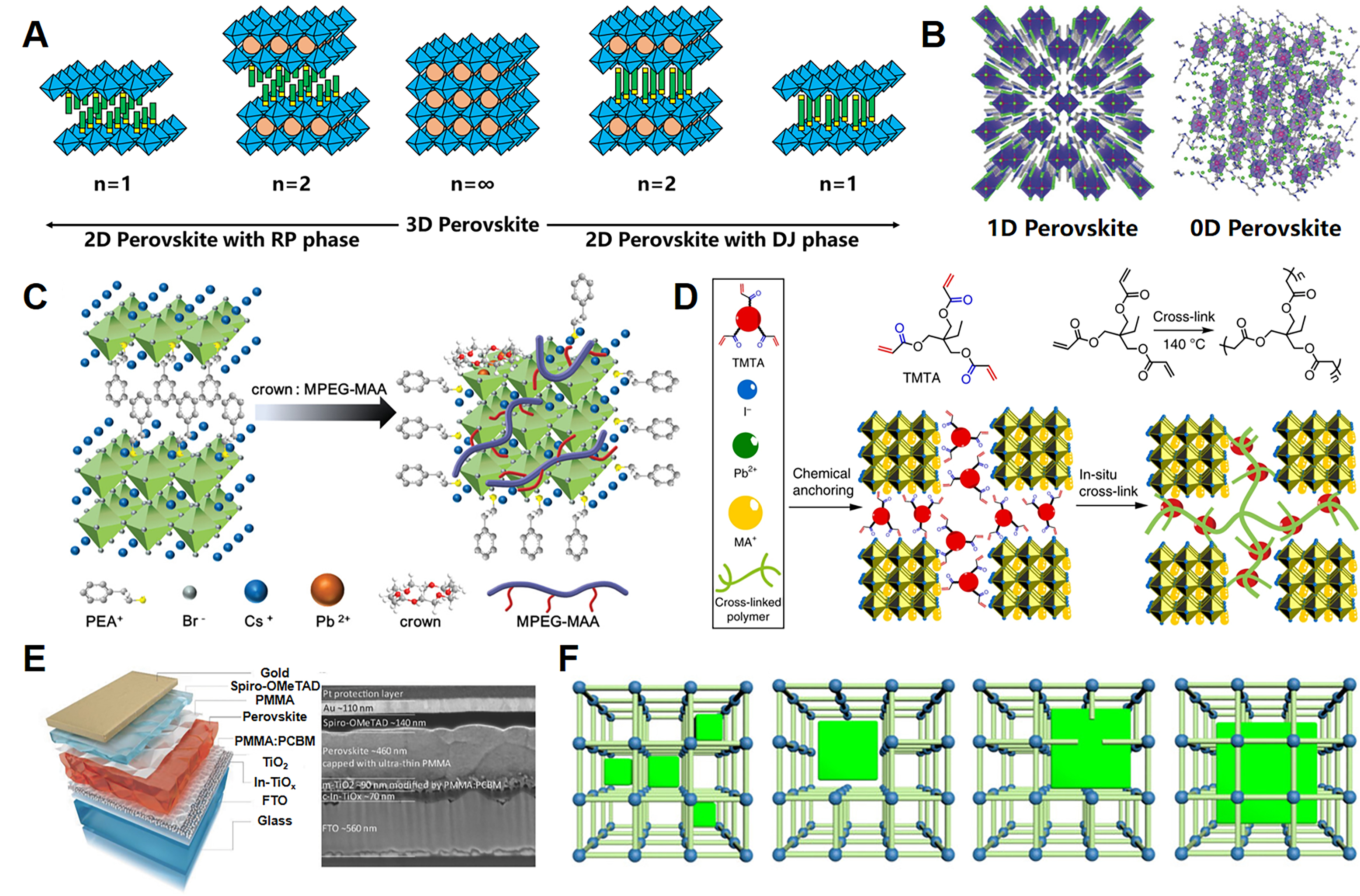
Figure 2. (A) Schematic diagram of crystal structures transformation from a 3D perovskite to 2D perovskites with RP and DJ phase, respectively. (B) Schematic illustrations of 1D and 0D perovskite structures[39]. (C) Schematic illustration of crystal structure change and defect passivation by crown and MPEG-MAA[48]. (D) Schematic diagram of in situ cross-linked organic/perovskite films[49]. (E) Schematic illustration of the device structure and corresponding SEM cross-sectional image[50]. (F) Schematic diagrams of ultrasmall perovskite quantum dots within micropore structure of MOFs, perovskite nanocrystals within mesopores or flexible pores of MOFs, perovskite nanocrystals throughout the pores of MOFs, and perovskite nanocrystals coated with MOF shells[16].