




fig1
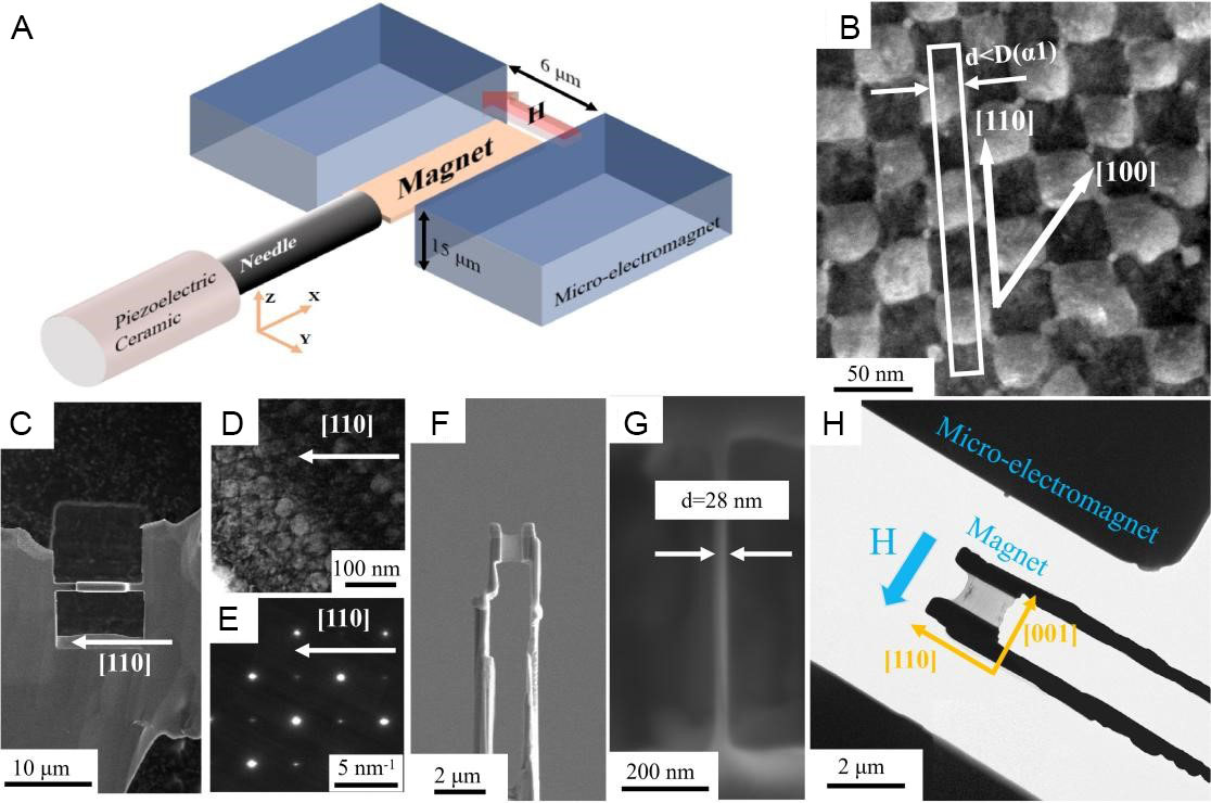
Figure 1. (A) Schematic of the in situ magnetic sample holder and SEM image of the microelectromagnet; (B) HAADF image of the Alnico alloy observed along the [001] direction, with the white box indicating the FIB sampling location; (C) SEM image of the FIB sampling area; (D) bright-field image of the FIB sampling area; (E) SAED pattern of the FIB sampling area; (F) SEM images of the samples used for in situ testing; (G) thickness of the observation area measured by SEM; (H) photograph of samples and microelectromagnets used in the In situ magnetization tests. SEM: Scanning electron microscopy; HAADF: high-angle annular dark field; FIB: focused ion beam; SAED: selected area electron diffraction.