


fig9
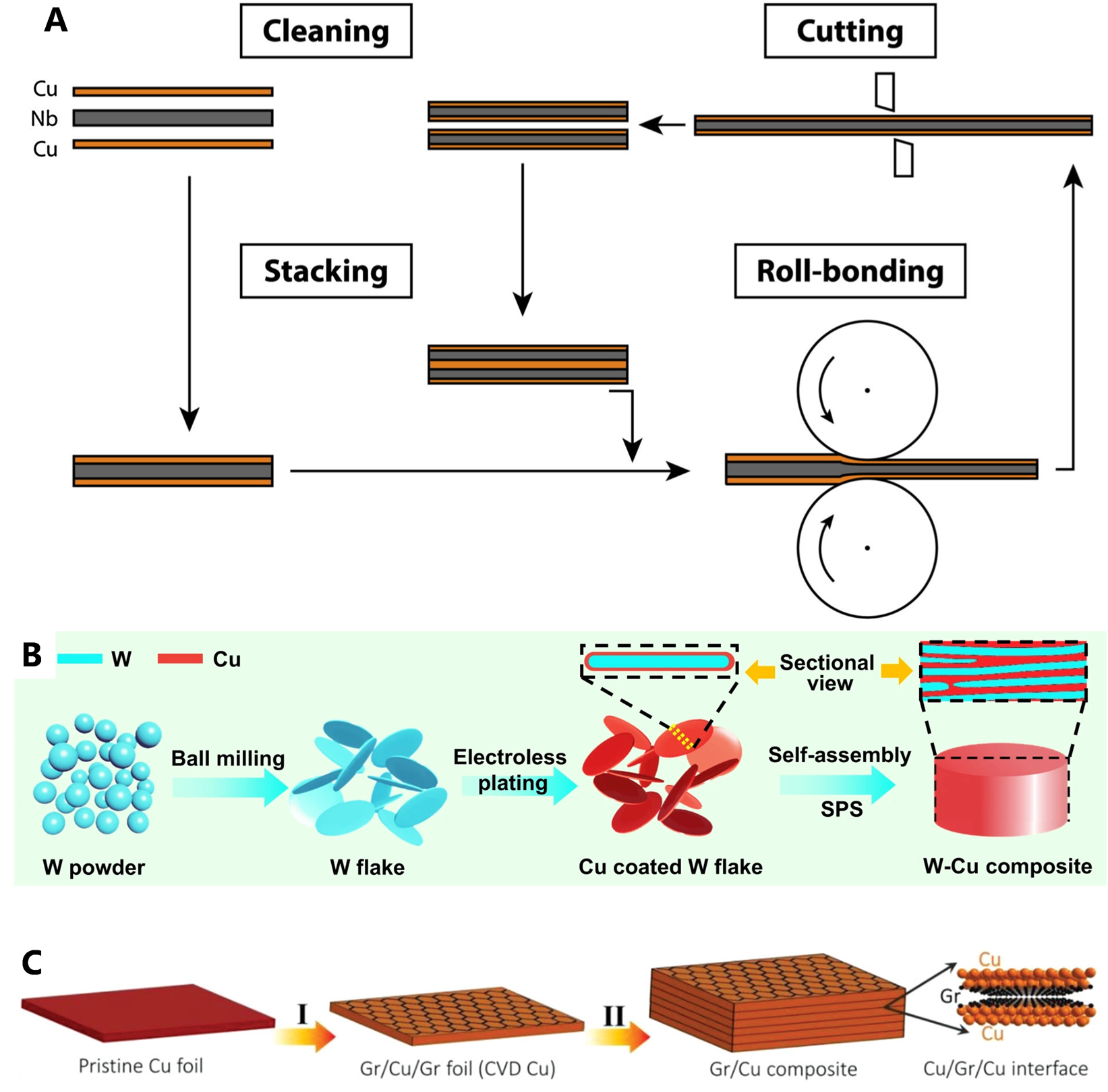
Figure 9. Processing methods for layered heterostructured copper alloys. (A) Schematic of ARB[87] (Reprinted from Ref.[87], with permission from Elsevier). (B) Schematic diagram of the design strategy for the W-Cu[90] (Quoted with permission from Han et al.[90], under the CC BY 4.0 license, http://creativecommons.org/licenses/by/4.0/). (C) Fabrication of Gr/Cu composites with aligned CVD graphene[95] (Reprinted from Ref.[95], with permission from John Wiley & Sons).


