

fig10
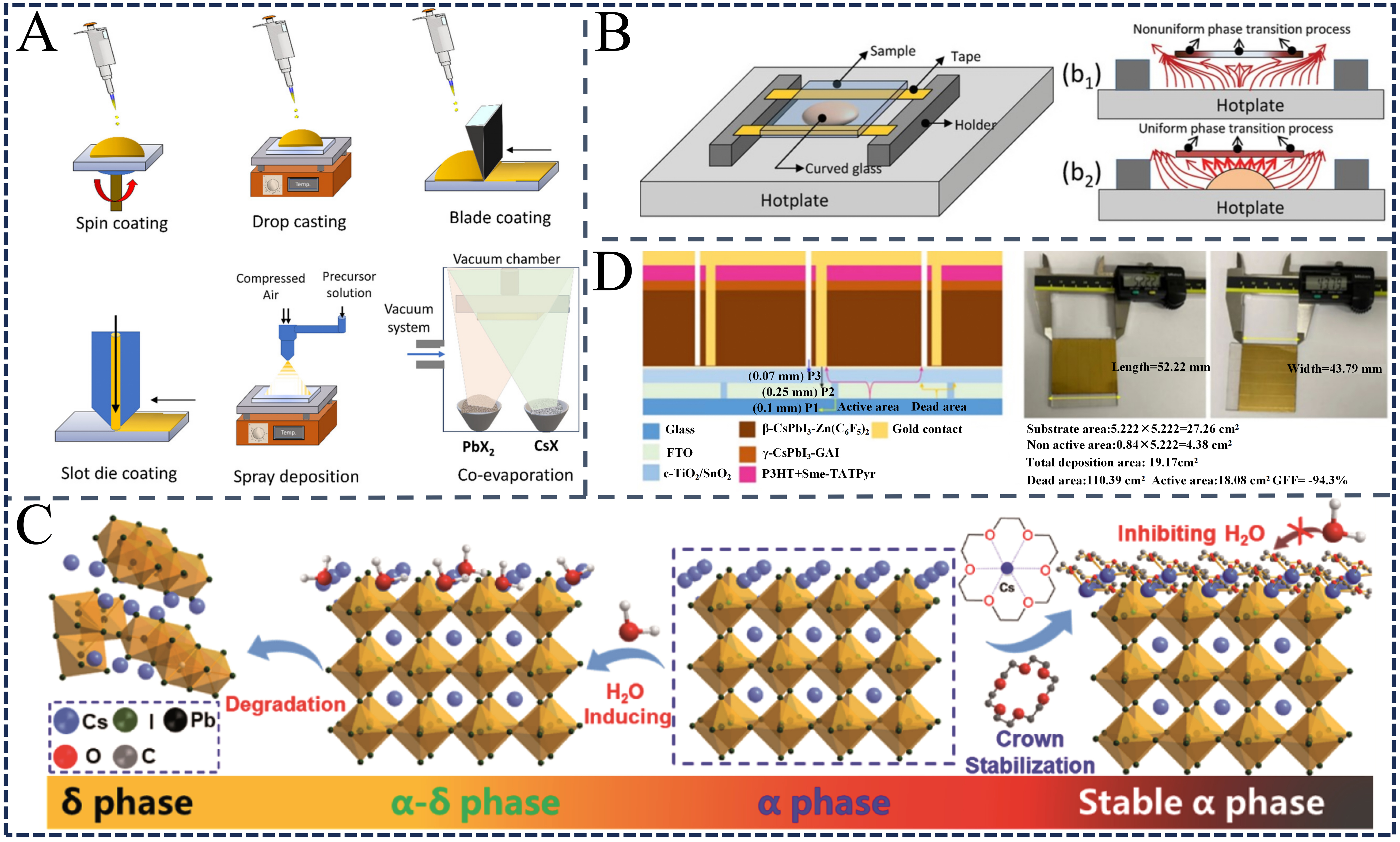
Figure 10. (A) A schematic diagram of a deposition method for large areas (≥ 1 cm2 × 1 cm2) inorganic devices. Reprinted from Ref.[63] under the CC BY 4.0 license; (B) A schematic diagram of preparing CsPbI2Br films on large-sized substrates using the quasi-curved heating method. This figure is quoted with permission from Ref.[198], Copyright © 2020 Wiley-VCH; (C) Schematic diagram of crown passivation on the surface of α-phase CsPbI3 and comparison with the phase transformation from α-phase CsPbI3 to δ-phase CsPbI3. This figure is quoted with permission from Ref.[199], Copyright © 2020 The Royal Society of Chemistry; (D) The left figure shows the schematic structure of the inorganic perovskite micro-module based on CsPbI3-Zn(C6F5)2/γ-CsPbI3-GAI, and the right figure is a photo of the module. This figure is quoted with permission from Ref.[200], Copyright © 2023 Springer Nature. GAI: Guanidine iodide.

