

fig2
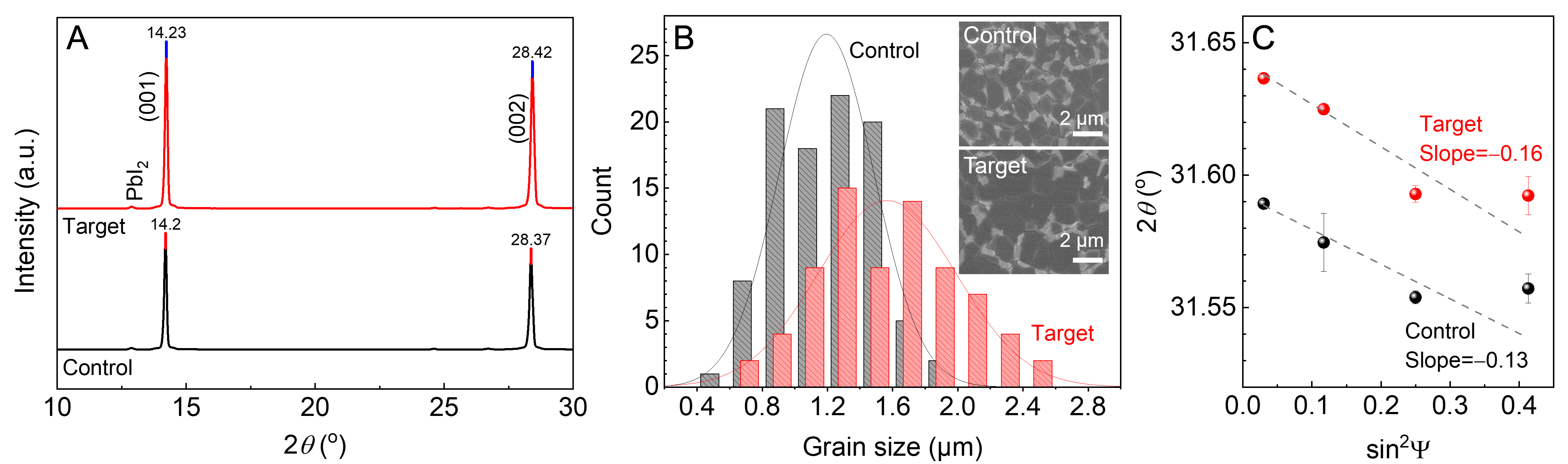
Figure 2. (A) XRD patterns and (B) grain-size distribution histograms of the control (black) and target (red) perovskite films. Insets in (B) show top-view SEM images of the control and target films; (C) 2θ-sin2Ψ plots of the control (black) and target (red) films obtained by GIXRD. Error bars represent the standard error of the fitted peak positions from a single measurement. XRD: X-ray diffraction; SEM: scanning electron microscopy; GIXRD: grazing-incidence X-ray diffraction.