


fig2
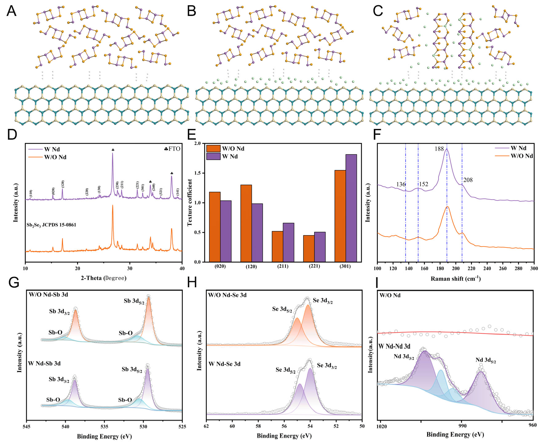
Figure 2. (A-C) Effect of W Nd-CdS and W/O Nd-CdS layers on the orientation of Sb2Se3 thin films, (D) XRD patterns of Sb2Se3 films with W Nd-CdS and W/O Nd-CdS layers, (E) Texture coefficients of Sb2Se3 films with W Nd-CdS and W/O Nd-CdS layers, (F) Raman spectra of Sb2Se3 films with W Nd-CdS and W/O Nd-CdS layers, (G-I) XPS spectra of Sb 3d, Se 3d, and Nd 3d for Sb2Se3 films prepared with


