
Time
10:00 AM, 3 December 2026 (Spanish, UTC+1)
5:00 PM, 3 December 2026 (Beijing, UTC+8)
9:00 AM, 3 December 2026 (UTC)
5:00 PM, 3 December 2026 (Beijing, UTC+8)
9:00 AM, 3 December 2026 (UTC)
Join the Forum
Platform: Zoom Meeting (with live streaming available)
ZOOM Meeting ID: 851 1474 0810
Link: https://us06web.zoom.us/j/85114740810
ZOOM Meeting ID: 851 1474 0810
Link: https://us06web.zoom.us/j/85114740810
Host
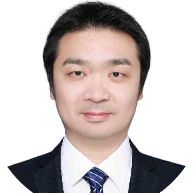
Yang Cao
School of Mechanics and Materials, Hohai University, China.
Prof. Yang Cao received his PhD degree from the University of Sydney in 2013. He is currently the Laboratory Manager of the Materials Characterization Center at Hohai University in Changzhou, China. Yang has long been dedicated to the study of microscopic deformation mechanisms and the regulation of mechanical properties in structural materials, as well as the development and application of in-situ transmission electron microscopy (TEM) techniques, EBSD/TKD data analysis techniques, and digital image correlation (DIC) techniques. He has published over 80 SCI-indexed papers, including more than 40 as the first or corresponding author, with over 6,500 citations and an h-index of 43. He has been granted 16 invention patents and is ranked among the world's top 2% of scientists. He serves as an Editorial Board Member of the international peer-reviewed journal Microstructures, and as a Young Editorial Board Member of Materials Research Letters and the Journal of Chinese Electron Microscopy Society.
Yang co-authored a highly cited review article entitled "Structural evolutions of metallic materials processed by severe plastic deformation" in Materials Science and Engineering: R: Reports, a journal with a 2023 Journal Impact Factor of 31.6. Yang was the first to propose a method for visualizing shear strain induced by high-pressure torsion in a dual-phase material. By employing this method to visualize shear strain, he observed phenomena such as stress concentration caused by inhomogeneous strain distribution and the gradual approach to an idealized state as shear strain increased. This work earned him the UFG VI Young Scientist Award at the 2010 TMS (The Minerals, Metals & Materials Society) Annual Meeting & Exhibition in Seattle, Washington, USA.
Yang was among the early researchers involved in the application of transmission Kikuchi diffraction (TKD) technology. In 2014, he co-authored a study demonstrating the application of TKD in a scanning electron microscope for characterizing deformed ultrafine-grained and nanocrystalline materials. Compared with conventional EBSD, TKD offers significantly improved spatial resolution, which can reach approximately 2 nm. Today, this technology is widely used in materials characterization.
Yang co-authored a highly cited review article entitled "Structural evolutions of metallic materials processed by severe plastic deformation" in Materials Science and Engineering: R: Reports, a journal with a 2023 Journal Impact Factor of 31.6. Yang was the first to propose a method for visualizing shear strain induced by high-pressure torsion in a dual-phase material. By employing this method to visualize shear strain, he observed phenomena such as stress concentration caused by inhomogeneous strain distribution and the gradual approach to an idealized state as shear strain increased. This work earned him the UFG VI Young Scientist Award at the 2010 TMS (The Minerals, Metals & Materials Society) Annual Meeting & Exhibition in Seattle, Washington, USA.
Yang was among the early researchers involved in the application of transmission Kikuchi diffraction (TKD) technology. In 2014, he co-authored a study demonstrating the application of TKD in a scanning electron microscope for characterizing deformed ultrafine-grained and nanocrystalline materials. Compared with conventional EBSD, TKD offers significantly improved spatial resolution, which can reach approximately 2 nm. Today, this technology is widely used in materials characterization.
Speaker

José María De Teresa
Nanofabrication and Advanced Microscopies (NANOMIDAS) Group, Instituto de Nanociencia y Materiales de Aragón (INMA), CSIC–University of Zaragoza, Spain.
Prof. José María De Teresa leads the Nanofabrication and Advanced Microscopies (NANOMIDAS) Group at the Institute of Nanoscience and Materials of Aragón (INMA), a joint institute of the Spanish National Research Council (CSIC) and the University of Zaragoza, Spain. He is the Coordinator of the FIB-SEM area at the Spanish National Facility for Advanced Microscopies (LMA) in Zaragoza. He coordinated the Spanish network on Nanolithography (NANOLITO) from 2005 to 2025. He served as Chair of the Board of the Condensed Matter Division of the European Physical Society (EPS) from 2021 to 2024. His main research interests are nanofabrication using focused electron and ion beams, magnetic nanostructures, nano-superconductivity, and quantum technologies. He has published 253 research articles, with 12,700 citations in Scopus and an h-index of 56, and has delivered more than 100 invited presentations at conferences. He has supervised 22 PhD theses. He is a Fellow of the American Physical Society (2021), a Fellow of the European Physical Society (2023), and a Fellow of the European Academy of Sciences (2024). He has served as President of the European Physical Society (EPS) since May 2026.
Abstract
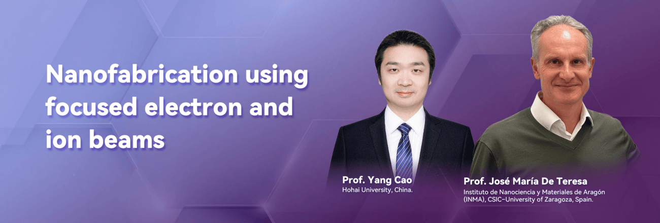
In this talk, I will review the results obtained by the Nanomidas group at INMA in the topic of nanofabrication using focused electron and ion beams, as well as its application to various topics in Physics and Materials Science. Focused electron beams are produced in a Scanning Electron Microscope (SEM) and are mainly used for imaging or for electron beam lithography, whereas the Focused Ion beam (FIB) is mostly popular for nanopatterning via the local removal of material. Interestingly, if one combines focused electron or ion beams with a precursor material, a local deposit can be grown, and the techniques are respectively named Focused Electron Beam Induced Deposition (FEBID) and Focused Ion Beam Induced Deposition (FIBID). The talk will describe the fundamentals of these techniques and a few examples of application in the fields of Magnetism, Superconductivity, Quantum Technologies and Nanoelectronics.
Keywords: nanofabrication, focused electron and ion beams, nanoelectronics, nanomagnetism, nanosuperconductivity, quantum technologies, microscopy
Keywords: nanofabrication, focused electron and ion beams, nanoelectronics, nanomagnetism, nanosuperconductivity, quantum technologies, microscopy