


Topic: Microstructure Engineering and Optoelectronic Properties in Low-Dimensional Semiconductor Materials
Guest Editors
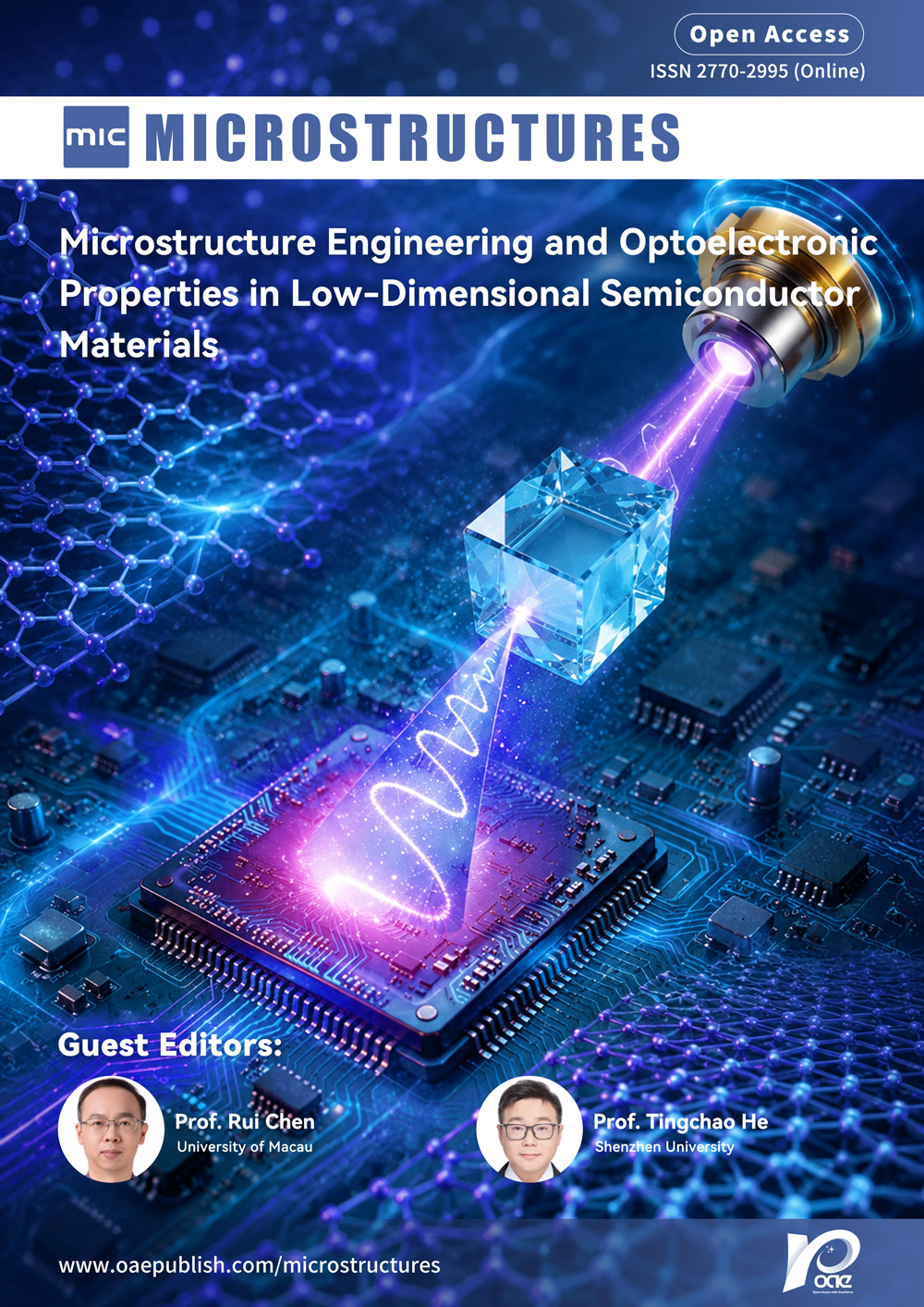
Special Topic Introduction
Low-dimensional semiconductor materials, including perovskites, quantum dots, two-dimensional materials, and related nanostructures, have attracted tremendous attention due to their outstanding optoelectronic properties and broad applications in light-emitting devices, lasers, photodetectors, and emerging quantum photonic technologies. Their performance, such as emission efficiency, charge transport, spectral tunability, and photoresponse, is strongly governed by microstructural characteristics, including defects, interfaces, grain boundaries, and dimensionality. Microstructure engineering has therefore emerged as a central strategy for tailoring and optimizing the optoelectronic properties of low-dimensional semiconductors. Precise control over crystallization processes, morphology, and interfacial structures enables improved carrier dynamics, enhanced radiative recombination, and suppressed non-radiative losses, which are essential for high-performance and stable optoelectronic devices.
This Special Issue focuses on recent advances in the design, characterization, and control of microstructures in low-dimensional semiconductor materials, with particular emphasis on their optoelectronic properties and underlying mechanisms. It aims to highlight fundamental insights into structure–optoelectronic property relationships, as well as innovative approaches for improving device performance, efficiency, and stability. Contributions covering experimental, theoretical, and computational studies are welcome.
Topics of interest include, but are not limited to:
● Modeling, simulation, and AI-assisted design for optoelectronic materials;
● Crystallization control and microstructure evolution;
● Defect, interface, and grain boundary engineering;
● Stability and degradation mechanisms;
● Light-matter interaction and optical gain in low-dimensional materials;
● Nonlinear optics and ultrafast spectroscopy of low-dimensional materials;
● Construction of chiral low-dimensional semiconductors and relevant applications
● Optoelectronic devices, including solar cells, photodetectors, synaptic devices, LEDs, and lasers.
Keywords
Low-dimensional semiconductor materials, microstructure engineering, defect engineering; Interface design, structure–property relationship, performance optimization.
Submission Deadline
Submission Information
For Author Instructions, please refer to https://www.oaepublish.com/microstructures/author_instructions
For Online Submission, please login at https://www.oaecenter.com/login?JournalId=microstructures&IssueId=microstructures26061710500
Submission Deadline: 31 Dec 2026
Contacts: Juno, Assistant Editor, [email protected]


